Recently, zinc oxide (ZnO) has been extensively investigated for its potential use to achieve high performance in short-wavelength light-emitting devices because of its large excitation binding energy of 60 meV and its direct wide energy band gap of 3.37 eV at room temperature. To implement light-emitting devices based on ZnO, it is of pivotal importance to grow p-type ZnO films for fabricating p-n junctions. Theoretically, N is the best p-type dopant for group V elements because its ionic radius is approximately equal to that of O [1]. Obtaining reproducible high-quality p-type ZnO films using mono-doping methods has always been an intractable and unresolved problem, and as a result, nitrogen mono-doped p-type ZnO films show low hole concentration,especially when the magnetron sputtering method is used [2,3].The N-type compensation effect induced by interstitial zinc (Zni)and oxygen vacancy (VO), low acceptor solubility, and deep acceptor levels are the main bottlenecks to obtaining p-type ZnO using the mono-doping method. Theoretically, codoping group V and III elements at a 2:1 ratio in ZnO can increase acceptor solubility and make acceptor levels shallower by reducing Madelung energy, solving the problems of p-type doping in ZnO [4,5].The theoretical feasibility of codoping has been demonstrated by experiments[2,6-8]. DC-magnetron sputtering has an advantage over RF- magnetron sputtering in that it uses electric power more effectively. Moreover, DC reactive magnetron sputtering has been successfully used for N-Al codoping of p-type ZnO films, resulting in enhanced hole concentration compared with mono-N doped p-type ZnO films [2,3]. However, in most cases, the p-type ZnO films prepared by this method have always showed low hole mobility (less than 3 cm2V-1s-1) when the p-type carrier concentration was greater than 1016 cm-3, which is the lowest practical value for optoelectronic devices [2,3,8-10]. In a previous study,the authors obtained p-type carrier mobility values ranging from 0.19 to 11 cm2V-1s-1 in ZnO:Al films using a ZnO:Al2O3 (2 wt%)ceramic target with pure oxygen ambient and the RF magnetron sputtering method [11]. In that paper, the scanning electron microscopy(SEM) image showed evident columnar structure, which means low structural quality. When DC magnetron sputtering is used to grow N-Al codoped ZnO films, metallic Zn mixed with a small fraction of metallic Al is usually used as a target. In the present study, Al-N codoped p-type ZnO films with high carrier mobility were first fabricated on n-type silicon substrates using a ZnO:Al2O3 ceramic target by DC magnetron sputtering.
ZnO films codoped with Al and N were deposited on n-type Si (100) (1-10 Ωcm) and homo-buffer layer templates by homemade DC magnetron sputtering. Ceramic ZnO (5N) and RF magnetron sputtering were used respectively as a sputtering target and a power supply for fabrication of a homo-buffer layer. The other conditions for deposition of homo-buffer layers on n-type Si (100) (1-10 Ωcm) were described in a previous study by the authors [12]. The ceramic ZnO mixed with 2 wt% Al2O3, which also acted as an Al source for codoping ZnO films, was selected as a sputtering target. The sputtering ambient was a mixture of N2 and O2 gases at ratios of 1:4, 2:3, 3:2 and 4:1 to implement codoped ZnO:(N,Al) films. Working pressure, DC power, growth temperature, and growth time were set to 6 and 15 mTorr, 340 V× 0.1 A, 450°C, and 90 minutes respectively to obtain a film thickness of approximately 450 nm. To evaluate p-type films further, a p-type Al-N codoped ZnO layer and a nominally undoped n-type ZnO layer were deposited on a p-Si (100) substrate sequentially to fabricate a p-n junction with top and bottom electrodes. X-ray diffraction (XRD) spectroscopy, field emission SEM, Hall effect determination in the Van der Pauw configuration, photoluminescence(PL) evaluation, X-ray photoelectron spectroscopy (XPS),and measurement of the I-V curve of a p-n junction were carried out to evaluate the microstructural, electrical, optical, and chemical properties of Al-N codoped films.
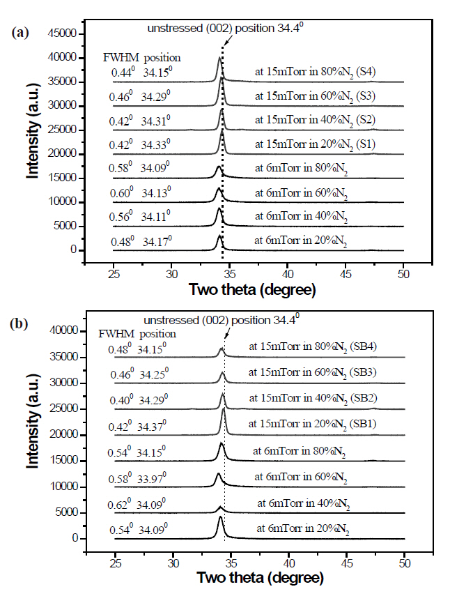
Figure 1 shows that all films have a predominant growth orientation along the c-axis of a hexagonal Wurtzite crystal ZnO structure, implying that DC magnetron sputtering is beneficial to the unidirectional growth of Al-N codoped ZnO. Two-theta diffraction(002) peaks lie at a position slightly below the unstressed position of 34.4°, revealing that the crystal c-axis lattice constant of the films is greater than that of single-crystal bulk ZnO. This can be ascribed to the presence of molecular N2 in the ZnO [12].The crystal c-axis lattice constant of films grown at 15 mTorr is closer to the corresponding lattice constant of bulk ZnO than that of films grown at 6 mTorr, regardless of the substrate, implying more incorporation of molecular N2 in the films grown at 6 mTorr. The full widths at half maximum (FWHMs) of (002) peaks at 6 mTorr are larger than those at 15 mTorr, which indicates that the average grain sizes of the films grown at 6 mTorr are smaller than of those at 15 mTorr. The intensity of the (002) peak of ZnO films grown on Si substrates at 15 mTorr is higher than that of films grown at 6 mTorr (Fig.1 (a)). However, the intensity of the(002) peak of films deposited on buffer-layer templates does not show a clear difference between films grown at 15 mTorr and
at 6 mTorr (Fig.1 (b)). Usually, the buffer layer is beneficial to the crystallinity and microstructure of the ZnO film, but in the case of Al-N codoped ZnO films deposited by DC magnetron sputtering and using ceramic ZnO:(Al2O3) as a target, the buffer layer does not create an improvement in the ZnO microstructure.These results are much different from those in the authors’previous study, in which Al-N codoped ZnO films were deposited on Si and on identical homo-buffer layer templates by RF magnetron sputtering. In that paper, by comparison to the films on Si, the crystallinity of films on homo-buffer layer templates showed a great improvement. More attention should be paid to the positions and FWHMs of (002) peaks of the films at 15 mTorr.The greater the N2 fraction in the N2-O2 mixture, the smaller is the value of the position and the larger is the FWHM, which indicates that more molecular nitrogen goes into the films and makes the grain size smaller.
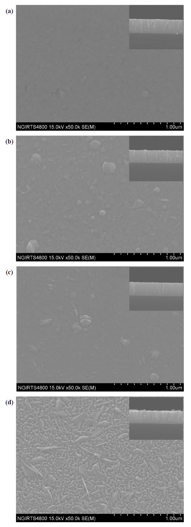
Figure 2 shows that over a broad range of low N2 fractions in the N2-O2 mixture (from 20% to 60%), the surfaces of codoped films have high smoothness. However, at a high N2 fraction of 80%, the surface of the codoped film has distinct textural features,and the average grain size is approximately 59 nm, which is approximately consistent with the value of 55 nm calculated from the FWHM of the XRD spectrum of the same sample using Scherer’s equation. The cross-sectional images in the insets in Fig. 2 show that films grown in moderate N2 fractions of 40% and 60% have a fairly smooth cross section. In a low N2 fraction of 20%, the cross-sectional image shows columnar characteristics.In a high N2 fraction of 80%, the cross-sectional image shows an evident columnar structure.
Hall effect measurement in the Van der Pauw configuration was carried out to evaluate the electrical properties of the films.Table 1 lists the electrical properties for films grown at 15 mTorr
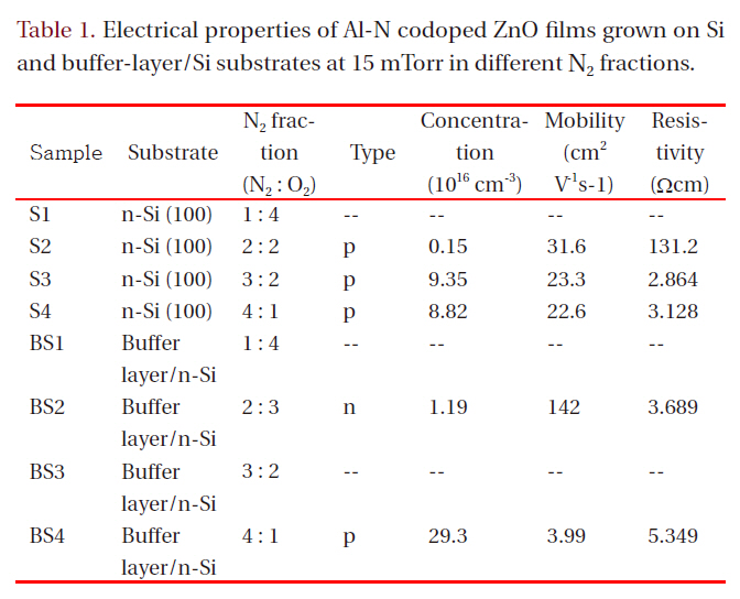
Electrical properties of Al-N codoped ZnO films grown on Siand buffer-layer/Si substrates at 15 mTorr in different N2 fractions.
in different N2 fractions. Samples S1, BS1, and BS3 had high resistivity (>1 × 10⁵ Ωcm), which was beyond the measurement range of the Hall-effect equipment used. All other Al-N codoped ZnO films on Si substrates showed p-type conduction. The hole mobility of the films grown on Si decreased with increasing N2 fraction in the ambient. However, the mobility values are all in excess of 20 cm2V-1s-1. These values are much higher than those of p-type films formed on a buffer layer in an N2 fraction of 80%(SB4). Although sample SB4 shows a high hole carrier concentration of 2.93 × 1017 cm-3, its hole mobility is only 3.99 cm2V-1s-1. The mobility values found in the present study are much higher than those obtained using metal Zn:Al as a target [3,7,9,10,13], implying that the ZnO:Al2O3 ceramic target has an advantage over the metallic Zn:Al target for obtaining high hole mobility in fabrication of Zn-Al codoped p-type ZnO films using DC magnetron sputtering. The hole concentration of films on Si increases from 0.15 × 1016 cm-3 for the film grown in 40% N2 to 9.35 × 1016 cm-3 for the film grown in 60% N2 and then decreases slightly for the film grown in 80% N2. The resistivity in the film grown in 60% N2 shows the lowest value, 2.864 Ωcm. In Tu et al. [14], N-doped ptype ZnO films were implemented using RF magnetron sputtering;the hole concentration decreased with increasing nitrogen fraction in an N2/Ar ambient, and the XRD patterns showed a zinc nitride phase. In the present study, the hole concentration does not decrease substantially with increasing nitrogen fraction in an N2/O2 ambient, and the XRD does not show zinc nitride,implying that N-Al codoped ZnO thin films grown by DC magnetron sputtering with a ZnO:Al2O3 ceramic target have higher quality than those formed by RF magnetron sputtering. Although in XRD patterns the films grown in a high N2 fraction show lower values of the (002) peak position than films grown in a low N2 fraction, which means high rates of molecular nitrogen incorporation into films, it is apparent from Table 1 that more atomic nitrogen is incorporates in filmd under condition of high nitrogen fraction in a growing ambient, which creates p-type films with a high carrier concentration.
When films were grown on buffer-layer templates, the conduction type changed from n-type to p-type with increasing N2 fraction in the gas mixture. The p-type film (BS4) grown on a bufferlayer template shows a high hole concentration of 2.93 × 1017 cm-3 and a low hole mobility of 3.99 cm2V-1s-1. The n-type film (BS2)grown on a buffer-layer template shows a low electron concentration of 1.19 × 1016 cm-3 and a high mobility of 142 cm2V-1s-1, which is high compared to reported values in the literature from the magnetron sputtering method. Low electron concentration is attributed to the action of atomic nitrogen as an acceptor in ZnO.
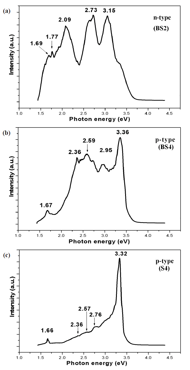
PL spectra of samples BS2, BS4, and S4 at 6 K are shown in Fig..3 Sample BS2 (n-type) shows near-band edge levels at 3.15 eV and deep defect levels at 1.69, 1.77, 2.09, and 2.73 eV (Fig.3 (a)).
Sample BS4 (p-type) shows near-band edge levels at 3.36 eV and deep defect levels at 1.67, 2.36, 2.59, and 2.95 eV (Fig.3 (b)).Sample S4 (p-type) shows near-band edge levels at 3.32 eV and deep defect levels at 1.66, 2.36, 2.57, and 2.76 eV (Fig.3 (c)). The films grown on a buffer layer show a much higher defect intensity than the films on Si, implying that the films grown directly on Si achieve much higher quality than those grown on a buffer layer. The mechanism of the near-band edge emissions at 3.15 eV for BS2 and 3.36 eV for BS4 cannot be confirmed. The nearband edge emission of 3.32 eV for p-type film on Si (S4) can be attributed to a transition of donor-acceptor levels.
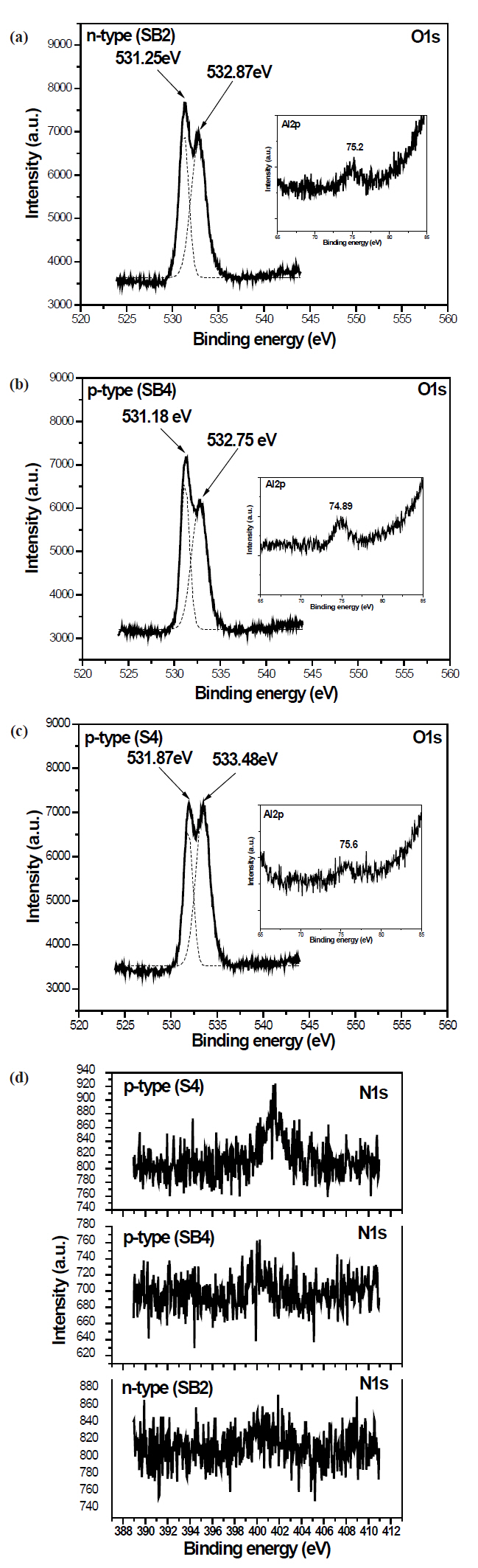
Figure 4 shows the XPS spectra of electron binding energies for O1s and Al2p. All O1s spectra show two peaks. The lower binding energy peak can be ascribed to Zn-O bonding in the normal ZnO structure and the higher to Al-O bonding [15]. All Al2p spectra show a peak at approximately 75 eV, higher than the 72.7 eV of metallic Al2p, which can be attributed to Al-O bonding. From Al2p spectra, all films do not possess an Al metallic state. This means that all the Al is in the Al-O and Al-N bonding states. XPS spectra of N1s for samples SB2, SB4, and S4 (Fig.4 (d)) exhibit peaks at a binding energy of approximately 400 eV, which is larger than that of AlN (397.5 eV) [16] and smaller than that of N1s in N-O bonds (407.6 eV) [10], which implies that the N is in the Al-N and N-O bonding states. The intensity of the p-type films is very evident, especially for sample S4, which implies that more nitrogen has been incorporated into the p-type films.
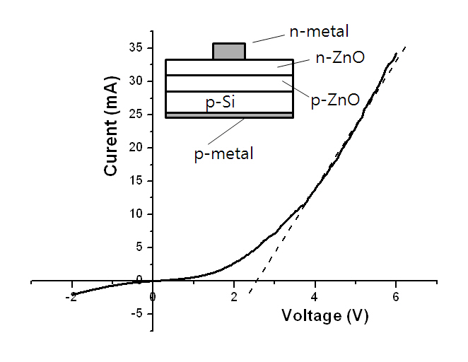
Figure 5 shows the I-V curve of a p-n junction with its structure in the inlet. The deposition conditions of the p-type ZnO layer were the same as those of sample S3 with a thickness of approximately 500 nm. The n-type ZnO layer was deposited in Ar at 15 mTorr and 300°C with a ZnO ceramic target using RF magnetron sputtering to obtain an electron concentration of approximately 2 × 1017 cm-3. The I-V curve shows a rectifying characteristic, and the turn-on voltage is approximately 2.6 V. The curve also shows a large leakage current which can be ascribed to the small grain size of the layers constituting the p-n junction.
In summary, Al-N codoped p-type ZnO thin films were deposited on n-type Si and buffer-layer templates with a ZnO:Al2O3 (2 wt%) target by DC magnetron sputtering method. All codoped films showed unidirectional growth along the crystal c-axis.High-quality codoped p-type conduction in films with high carrier mobility (over 20 cm2V-1s-1) can be obtained on Si. PL spectra at 6 K showed that high-quality codoped p-type ZnO:(N,Al) film can be obtained on Si in a high N2 fraction using DC magnetron sputtering. Oxygen was in the Zn-O and Al-O bonding states, and all aluminum was in the Al-O and Al-N bonding states. The I-V curve of the p-n junction showed a rectifying characteristic and a turn-on voltage of 2.6 V. From the I-V curve, it was evident that the condoped film on Si was of the p-type.