Nanocrystalline cadmium sulphide (CdS) is one of the attractive semiconductor materials and has been investigated for electronic and optoelectronic devices. Recently, Ghosh et al. [1] reported the field-emission properties of nanocrystalline CdS thin films grown by the chemical bath deposition (CBD)process within the pores of polyvinyl alcohol on Si and glass substrates. The solar cells of CdS/CdTe [2,3] and Cu(In,Ga)Se2(CIGS) [4,5] have been researched to increase the efficiency of cells. CdS thin films are prepared by vacuum evaporation [5-7],sputtering [2,8], screen printing [7,9], chemical pyrolysis [10],and CBD [1,3-5,7].
Among the various techniques, CBD is a simple and inexpensive solution deposition technique, in which thin film is prepared by chemical reaction in the solution bath. Also, it is possible to obtain uniform films with good adherence [11]. CBD CdS thin films are prepared by the decomposition of thiourea(SC(NH2)2) in an alkaline solution containing a cadmium salt,such as cadmium chloride (CdCl2), cadmium sulphate (CdSO4)and cadmium acetate (Cd(CH3COO)2). In the CBD technique for CdS thin films, the cadmium sulphate, thiourea and ammonium hydroxide serve as the cadmium source, sulphur source and complexing agent, respectively. CBD CdS thin films are prepared by the reaction of Cd2+ complex with S2-. Sulphur ions are supplied by the decomposition of thiourea in an alkaline solution,and cadmium ions are usually complexed by NH4OH [12].
The structural and optical properties of CBD CdS thin films depend on the parameters of relative concentration of the reactants for chemical reaction, pH value of the aqueous solution and bath temperature. The CdS thin films are deposited by the heterogeneous reaction on the glass substrate at low tempera-
ture. In the CBD process, film growth occurs either (i) by an ionby-ion condensation or (ii) by adsorption of the colloidal particles of CdS on the substrate [13]. The chemically deposited CdS film was found to consist of a continuous film relating to the ion-by-ion deposition of CdS [14]. The structural informations of CdS thin films such as crystal structure, interplanar distance and lattice constant are determined by the X-ray diffraction(XRD). The optical parameters of optical absorption coefficient and optical band gap are important to design the optoelectronic devices.
In this study, nanocrystalline CdS thin films were deposited on glass substrates by CBD. The structural, optical and photoconductive properties of CdS thin films were investigated. The crystal structure was studied using the XRD. Also, the Urbach energy, optical band gap, activation energy and photoconductive characteristic of CdS thin film were investigated.
CBD CdS thin films were deposited in an alkaline solution bath containing a cadmium salt, chalcogenide source and complexing agent. The alkaline solution of 0.5 M CdSO4, 1 M SC(NH2)2 and 25-28% NH4OH was used to prepare nanocrystalline CdS thin films by CBD. The CdS thin films were deposited on cleaned glass substrates. The alkaline solution bath was maintained at 80°C, and the pH value of the aqueous solution was 10. The glass substrates were washed in distilled water and ultrasonically cleaned subsequently in acetone, trichloroethylene and methanol. Then, the substrates were rinsed in deionized water and dried in an oven after N2 blowing. The preparation of CBD CdS thin films is based on the slow release of Cd2+ and S2-ions in the solution bath. The Cd2+ ions are given by the dissociation of a complex species of cadmium [Cd(NH3)4]2+. The S2- ions are obtained by the decomposition of thiourea (SC(NH2)2) in an alkaline solution, and react with [Cd(NH3)4]2+ ions to form CdS thin film [15,16]. The CdS thin films were prepared by taking out the glass substrates in a bath at different deposition times from 30 to 120 minutes. The deposited CdS thin films were rinsed in deionized water and cleaned ultrasonically. Then, the CdS thin films were dried in air.
The thickness of CdS thin films was measured by an ellipsometer(L116SF; Gaertner Scientific Co., Skokie, IL, USA). The surface morphology and cross-section of CdS thin films were
studied using a field emission scanning electron microscopy (FESEM)(JSM-6700F; Jeol Ltd., Tokyo, Japan). The crystal structure of CdS thin films was studied by XRD using an X-ray diffractometer(X’pert-APD; Philips, The Netherlands) with Cu Kα radiation(λ = 1.5406 A) at 40 kV and 30 mA. The optical transmission of CdS thin films was measured using a UV-VIS-NIR double beam spectrophotometer (CARY 5G; Varian Inc., Palo Alto, CA, USA) in the wavelength range 350-2,000 nm. The electrical conductivity and photocurrent of CdS thin films were investigated using the DC two probe method. Coplanar In/Ag electrodes for electrical and photoconductive measurements were deposited on CdS thin films by vacuum evaporation. To obtain ohmic contact, the electrodes were annealed at 150°C in N2 atmosphere for 5 minutes.The dark current and photocurrent of CdS thin film were measured by an electrometer/high resistance system (6517; Keithley Instruments Inc., Cleveland, OH, USA). The light source was a halogen lamp, while the light intensity was measured by a digital luxmeter.
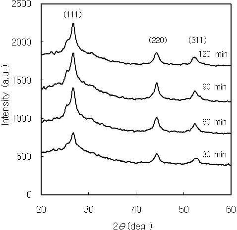
In the CBD CdS thin films, the morphology, structural and optical properties depend on the deposition parameters. The CdS thin films prepared by CBD have hexagonal or cubic polycrystalline structure. Cubic CdS grows in the zincblende structure, considered a metastable phase; hexagonal CdS grows in the wurtzite structure, which is the stable phase of the semiconductor [17].The as-deposited nanocrystalline CdS thin films had a cubic structure. The XRD patterns of CdS thin films are shown in Fig.1. Three diffraction peaks correspond to (111), (220), and (311)reflections of the cubic phase at 2Θ of 26.5°, 44° and 52°, respectively.The crystallite size of CdS thin films is determined by the Scherrer formula [18]. The crystallite size of CdS thin film prepared for 60 minutes was 7.2 nm. The crystallite size calculated using the full width at half maximum of the peak from the XRD is smaller than those calculated using absorption spectra. This is considered by the fact that the CdS particles are the aggregation of CdS nanoparticles [19] .
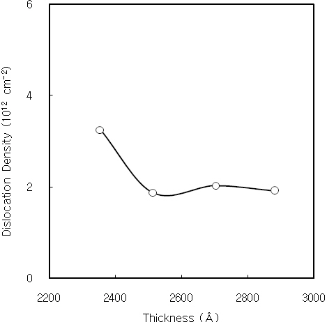
If the crystallite size is known, then the dislocation density of CdS thin films is obtained using the crystallite size [20]. Figure 2 shows the dislocation density of CdS thin films as a function of film thickness. It initially decreases with increasing the film
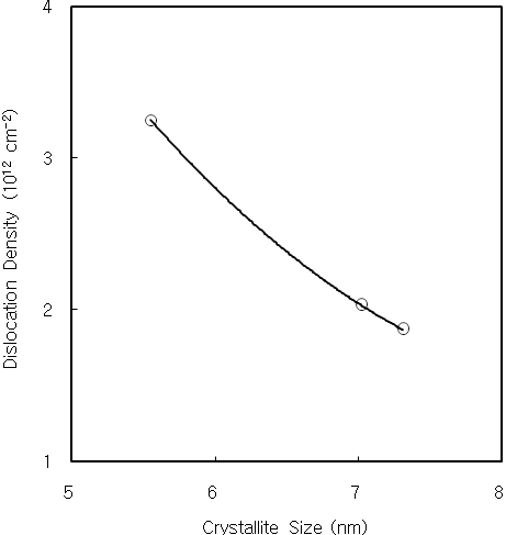
thickness, and it is nearly constant over the thickness of 2,500 A.It is considered by the decrease of internal strain with increasing the film thickness. Figure 3 shows the dislocation density of CdS thin films as a function of the crystallite size. The dislocation density decreases with increasing the crystallite size. Also, the interplanar distance and lattice constant of CdS thin films are obtained from the XRD data. The interplanar distance and lattice constant of CdS thin film prepared for 60 minutes was 3.35 A and 5.81 A, respectively.
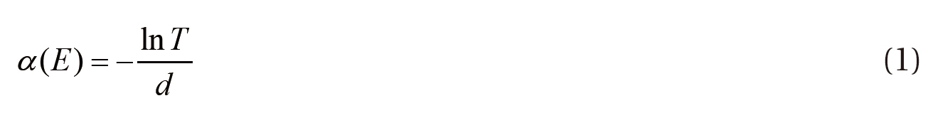
To obtain the optical absorption coefficient, the transmittance of CdS thin films was investigated. The optical absorption coefficientα(
where
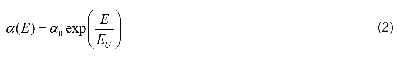
where αo is a constant, E is the photon energy and EU is an Urbach energy.
The Urbach energy characterizes the slope of the exponential edge region, and the inverse of the slope gives the width of the localized states associated with amorphous state in the band gap[23]. EU value that determines the steepness of the Urbach tail depends on the structural disorder of sample [24]. The Urbach energy EU is given as Eq. (3) [25].
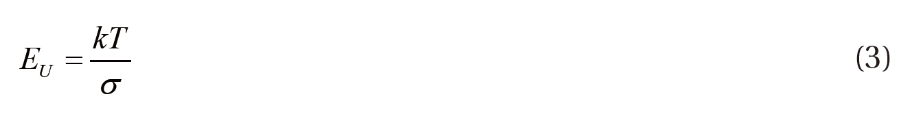
where σ is steepness parameter,
ting an exponential function to the slope of the linear portion of ln α vs.
The relation between the absorption coefficient and α energy of incident light
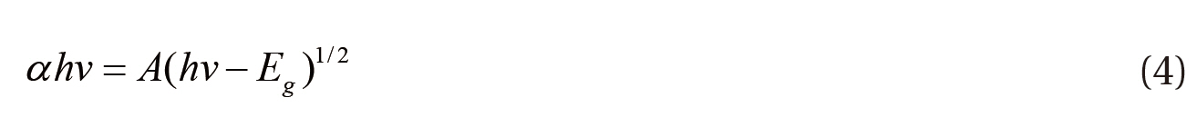
where
The activation energy

where σd is dark conductivity at temperature
is absolute temperature. Electrical conductivity was measured by using the DC two probe method.
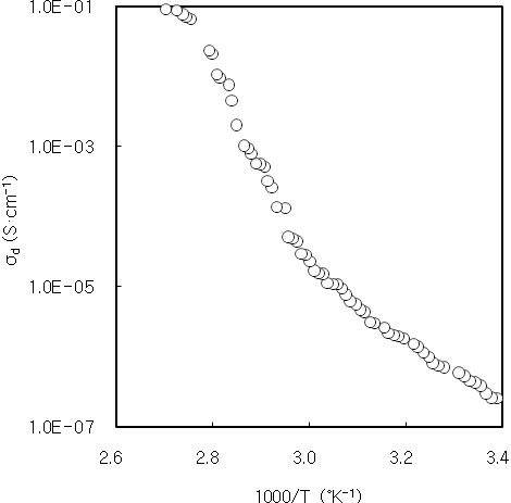
The temperature dependence of the dark conductivity of CdS thin film was composed of two regions as shown in Fig. 7. The dark resistivity of 2,900 A-thick CdS thin film at room temperature was of the order of 106 Ωcm. The high resistivity of CdS thin film is attributed to the nanocrystalline nature, dislocations and defects of the film [27]. The activation energies of the 2,900A-thick CdS thin film at low and high temperature regions were 14 meV and 31 meV, respectively. It is considered that these activation energies correspond to donor levels associated with the shallow traps or surface states of CdS thin film. The low activation energy of 14 meV at low temperature region was nearly the same as the value of
The photocurrent
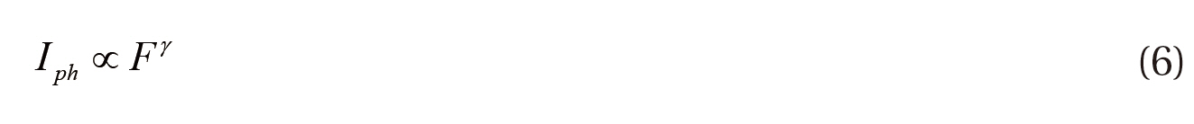
where
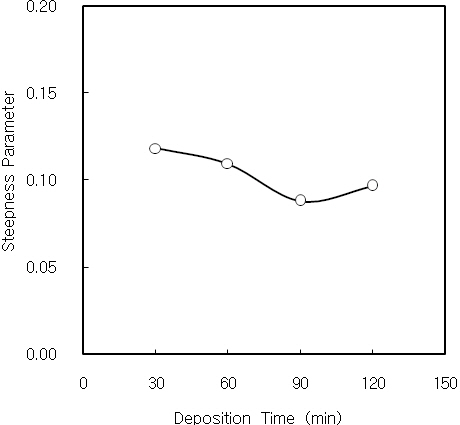
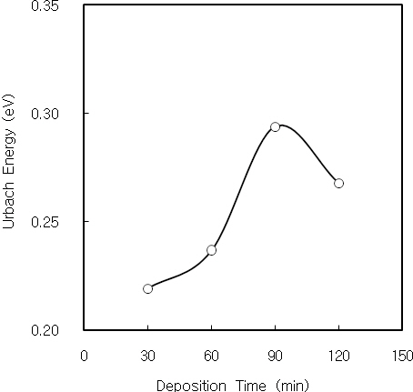
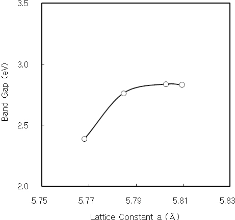
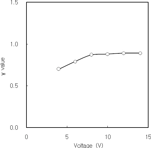
Nanocrystalline CdS thin films were deposited on cleaned glass substrates by CBD. The structural, optical and photoconductive properties of CdS thin films were investigated. From the XRD measurement, three diffraction peaks correspond to (111), (220) and (311) reflections of the cubic phase at 2Θ of 26.5°, 44°and 52°, respectively. The dislocation density of CdS thin film initially decreases with increasing the film thickness, and it is constant over the thickness of 2,500 A. It is considered by the decrease of the internal strain with increasing the film thickness.Also, the dislocation density decreases with increasing the crystallite size. The Urbach energies of CdS thin films deposited above 90 minutes are higher than the films deposited below 60 minutes. It is known that the quality of CBD CdS thin films is related to the deposition time and film thickness. The optical band gap of CdS thin films increases and finally saturates with increasing the lattice constant. The electrical conductivity and photocurrent of CdS thin film were investigated using the DC two probe method. The activation energies of the 2,900 A-thick CdS thin film at low and high temperature regions were 14 meV and 31 meV, respectively. It is considered that these activation energies correspond to the donor levels associated with shallow traps or surface states of CdS thin film. On the other hand, the 2,900A-thick CdS thin film has a bandgap of 2.83 eV, in which sulphur vacancies create shallow donor levels 14 meV and 31 meV below the conduction band. Also, the value of γ for the 2,900 A-thick CdS thin film was 1 at 10 V, and it saturates with increasing the applied voltage.