Aluminium gallium nitride (AlGaN)/GaN high electron mobility transistors (HEMTs) are a promising candidate for high power and high frequency applications due to their superior material properties [1,2]. Leakage current and premature breakdown not only degrade the blocking capabilities of power devices but also cause power losses in the system [3]. The active region leakage current is attributed to the electrons injected through the rectifying contact. In a lateral power device, the electron injection is mainly due to the strong electric field concentrated in the depletion region under the gate electrode compared to other factors [4]. In order to achieve stable blocking characteristics,such as low leakage current and high breakdown voltage, the peak intensity of the electric field at the gate depletion needs to be reduced. Our work concentrated on an investigation into the field modulation effect caused by implanted fluoride ions as well as the influence of the modified internal field on the blocking characteristics of an AlGaN/GaN HEMT. An improved blocking capability was confirmed by the measured leakage current and the breakdown voltage of the fabricated device.
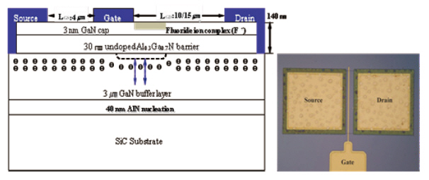
2. DEVICE STRUCUTURE AND FABRICATION
AlGaN/GaN heterostructure was grown on SiC substrates using metal organic chemical vapor deposition. A 30 nm-thick unintentionally doped Al0.3Ga0.7N and n 3 ㎛-thick GaN buffer formed the two dimensional electron gas (2DEG) channel of the AlGaN/GaN HEMT. An undoped GaN capping layer was then grown. A mesa structure with the thickness of 140 nm was formed for device isolation using the inductively coupled plasma
reactive ion etching (RIE) apparatus. In order to create the source and drain electrodes, a Ti/Al/Ni/Au (20/80/20/100 nm) based ohmic contact was e-gun evaporated then annealed at 870°C for 30 seconds under N2 ambient. A Ni/Au (30/150 nm) based Schottky contact was also e-gun evaporated. The standard lift off method was used to define these metallization patterns. Crosssectional view of the fabricated device was shown in Fig. 1.The device was then annealed at 500°C for 5 minutes under O2 and N2 ambient. A selective fluoride plasma treatment using a capacitive coupled plasma RIE apparatus was performed on the drainside gate edge region with selected radio frequency (RF) power conditions (from 15 to 60 W) for 120 seconds. The flow rate of the CF4 gas was set to 20 sccm at a pressure of 50 mT. The plasma treatment condition used for the device fabrication was greatly attenuated in order to minimize the surface damage. Through auger electron spectroscopy (AES) measurement, it was confirmed that fluoride atoms were implanted into the AlGaN layer.
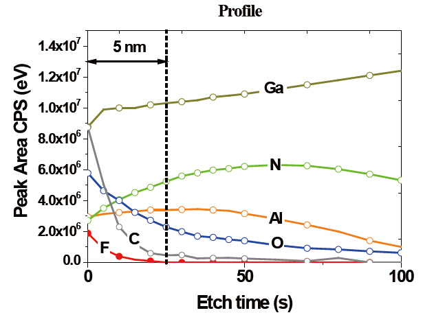
Fluoride atoms were implanted into AlGaN barrier layer through soft etching. The depth of the fluoride atoms was controlled by the plasma power to not invade the channel. As shown in Fig. 2, the fluoride atoms were distributed to within 5 nm from the AlGaN surface, considering the profiling time of the AES measurement. Most of these atoms were detected at the surface of the AlGaN layer. The concentration of fluoride ions decreased rapidly along the depth of the device.
The fluoride atoms implanted into barrier layer performed as negatively charged ions due to their strong electron affinity [5-7]. The implanted fluoride ions inhibited polarization charges from being induced at the AlGaN surface (negative polarization charge, -ρPZ) and at the AlGaN/GaN interface (positive polarization charge, +ρPZ) by an electrostatic interaction with the identical dipole arrays in the AlGaN layer.
Generally in the AlGaN layer, the polarization field is induced by the negative and positive polarization charges localized at both sides of the AlGaN layer. The polarization charges are introduced by the heads and the tails of the dipole array. The polarization is reinforced by a strain (tensile stress) in the AlGaN layer,whereas the polarization in the GaN layer is not. The discrepancy in the polarization is reflected in the difference of the internal field between the AlGaN and GaN layer. Due to this difference in the internal field, an electron channel (or 2DEG) is formed at the interface to offset the discrepancy [8,9]. In the plasma treated AlGaN layer, however, the negatively charged fluoride ions prevented the anions and cations from forming an electric dipole system through an electric repulsion force. A stack of disrupted dipole arrays has great difficulty in inducing the polarization charges at both ends of the stack. The polarization field in the plasma treated AlGaN layer was smaller than that found in a conventional HEMT. The difference in the field between the barrier
and buffer layer was also reduced. The electrons induced to form an equilibrium state (charge neutrality condition) at the AlGaN/GaN interface were decreased. The discrepancy of the field between the two layers was inversely proportional to the RF power.In the case of hard plasma treatment, where high RF power and long process times are used, there is no need for the electrons to be induced at the interface to compensate for the discrepancy.As a result, the channel of the AlGaN/GaN HEMT fabricated with a hard plasma treatment is fully depleted. The device operates in the enhancement-mode.
In this experiment, however, a soft plasma treatment was used in order to minimize the loss in the forward current and change the depletion region to be suitable for a stable blocking capability.The degree of the field modulation in the barrier layer was elaborately controlled by minute RF variations (15/30/45/60 W).In the soft plasma treated device, the polarization field was moderately modulated. This not only partially depletes the carriers in the channel but makes the depletion region more extended than before. A series of vertically expanded depletion regions was formed along the drift region by the fluoride plasma treatment.The expanded depletion region induced by the plasma treatment made the whole contour of the depletion region near the gate electrode sufficiently enlarged to sustain a high reverse bias.
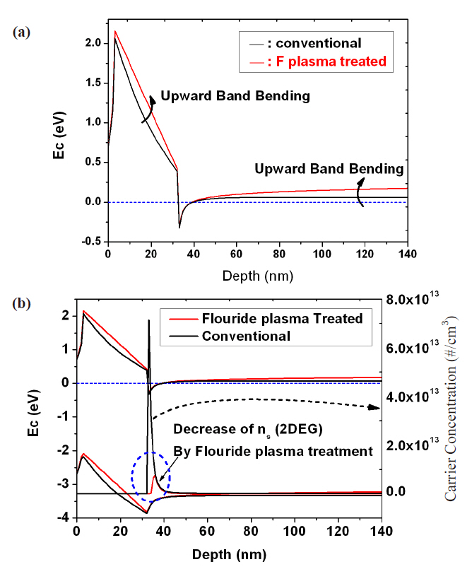
The modification of the internal field and depletion contour was confirmed by an upward band bending in the simulated energy band structure (Fig. 3) [10].
As shown in Fig. 3(a), the gradient of the potential (energy band) of the plasma treated device is relatively shallow at the AlGaN and GaN region, whereas that of the conventional one is steep at both regions. According to the Poisson equation, the gentle gradient of the potential indicates that a low electric field is induced at both layers. As the slope of the potential at both regions become more gradual, the depth of the quantum well formed at interface becomes shallow. It is directly related to the decrease of the carrier density, as shown in Fig. 3(b). In addition,the expansion of the depletion region in the GaN is confirmed in the simulated band structure. The depletion which plays a significant role in the reverse operation mode is the one formed in the GaN buffer layer rather than that formed in the AlGaN layer. In AlGaN/GaN HEMTs, it is defined as the length from the interface and the plateau of the band. As shown in Fig. 3(a), the depletion depth of the proposed device is much deeper than that of a conventional HEMT without any reverse bias.
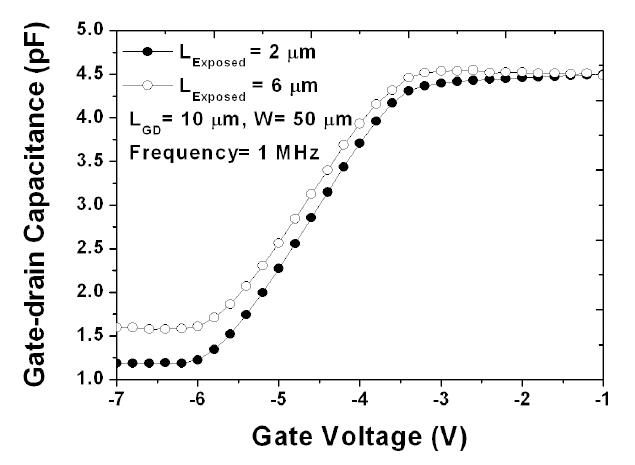
The change of the depletion was verified from the measured
C-V characteristic (Fig. 4), particularly from the measured offstate gate drain capacitance. For ease of understanding, a simplified equivalent capacitance model was used. The equivalent capacitance between the gate and drain can be simplified as a parallel connection between the capacitance of the capping layer and the series of the two AlGaN capacitances and the channel capacitance. The approximate equation for the gate-drain capacitance is:

Under a reverse bias condition, the gate bias is lowered below the pinch-off voltage. The channel capacitance (Cch) is equivalent to the depletion capacitance (Cdep). Eq. (1) can therefore be simplified. The resulting equation for the off-state gate drain capacitance under blocking mode is:

In Eq. (2), the capacitance of the GaN capping layer (Ccap) is fixed. The gate drain capacitance entirely depends on the depletion capacitance.
The area exposed to the plasma treatment was increased from 100 to 200 ㎛2; the off-state capacitance was increased from 0.119 to 0.160 pF. The increase in the off-state capacitance indicates that the area of the depletion capacitor was increased.In terms of the device, it means that a lateral expansion of the depletion occurred. The dilated depletion alleviated the field concentration at the gate depletion by distributing the electric field flux into an extra depletion region induced by the plasma treatment. Consequently, the electric field caused by a reverse bias was spread more uniformly in the drift region than before.The field intensity at the unit area of the gate depletion was thereby decreased.
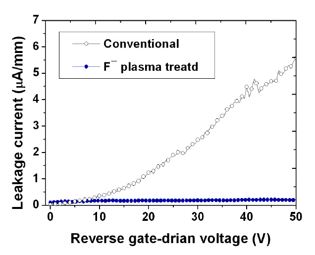
The leakage current was measured under the reverse bias condition where the gate and drain voltage was -7 V and 50 V,respectively. As field intensity at the gate depletion reduced, the probability that electrons would be injected into the barrier layer was decreased. The suppression of the electron injection led to a decrease in the leakage current. As shown in Fig. 5, the leakage current of the untreated device was 0.28 μA (current density: 5.6μA/mm), whereas that of the plasma treated HEMT was 9.5 nA(current density: 190 nA/mm).
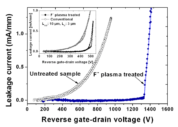
The breakdown characteristics of the fluoride plasma treated AlGaN/GaN HEMT was also investigated. As shown in Fig. 6, the breakdown of the conventional device occurred at 900 V; it showed soft breakdown characteristics. The breakdown of plasma treated device (at an RF power of 30 W) occurred at 1,400 V;it showed hard breakdown characteristics where leakage current was suppressed effectively right up to the breakdown regardless of reverse bias. It was reflected in both the suppression of leakage current and the improvement of breakdown voltage that the field modulation caused by the fluoride plasma treatment dropped the peak intensity of the electric field by introducing an additional depletion region near the gate electrode. The reliable blocking characteristics obtained by the fluoride plasma treatment guarantees a high power-handling capability for the device and a small power loss in the system.
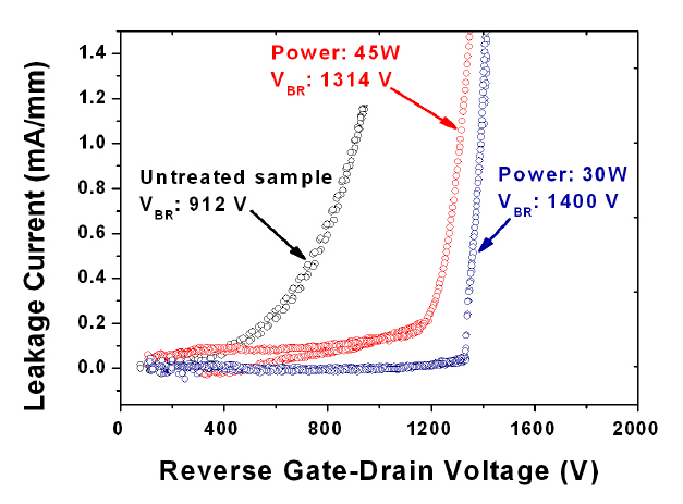
The blocking capability of the plasma treated device was im-
proved in proportion to the RF power until 30 W (Fig. 7). At RF powers higher than 30 W, however, the blocking characteristic was degraded in proportion to the RF power increase. Although the breakdown voltage of the device plasma treatment at the power of 45 W was over 1300 V, its reverse operation was more unstable than that found in the device plasma treated at 30 W.The leakage current of the devices plasma treated at RF powers over 30 W was influenced by the reverse bias and relatively high.The leakage current dependency on the reverse bias increased as the RF power increased. The breakdown voltage of the device treated at 60 W was similar to that of a conventional HEMT (not shown in Fig. 7). The leakage current was slightly higher than that of a conventional HEMT. At the plasma power over 30 W, the side effects caused by the plasma treatment outweighed the field modulation effects. To be more specific, at a high plasma power,the surface leakage current due to plasma damage overwhelmed the stable blocking operation established by the field modulation effect. Therefore, the device failed to operate stably in the reverse blocking mode irrespective of the field modulation effect.
We investigated the effect of the field modulation effect caused by implanted fluoride ions as well as the influence of the modified internal field on the blocking characteristics of AlGaN/GaN HEMTs. The fluoride plasma treatment expanded the gate depletion region laterally. This reduced the peak of the electric field concentrated at the gate edge by distributing the electric field more uniformly. Through this mechanism, the fluoride plasma treated device achieved a high breakdown voltage. The measured breakdown voltage of the plasma treated AlGaN/GaN HEMT was 1.4 kV. It was higher than that found for an untreated device by 55%.