Amorphous Si (a-Si) thin-film transistors (TFTs) are widely used as switching devices for active-matrix liquid-crystal displays (AMLCD) due to their many advantages such as low cost and efficient mass production. Based on the success of a-Si, a-Si TFT has been intensively investigated for realizing a future activematrix light-emitting diode (AMOLED) display [1,2]. However, a-Si TFT is not ideally suited for applications, such as AMOLED backplanes, unlike the case of AMLCD. It is known to be mainly due to low mobility and TFT instability [3-6]. Some reporters have revealed that microcrystalline Si (μc-Si) TFTs could be a good alternative [7]. The μc-Si TFT is compatible with the a-Si manufacturing technology in terms of having a well-established manufacturing infrastructure. The performance of μc-Si TFT is expected to have much higher field effect mobility [8]. Additionally, the stability of μc-Si TFT is improved under the DC bias stress [9]. However, the μc-Si has a relatively slow deposition rate, which is problematic for achieving efficient mass production. To address these problems, a bottom-gate TFT was proposed with an amorphous/μc-Si double layer (DL) as an active layer.
In this study, DL TFTs were fabricated and the variations of electrical characteristics were investigated according to direct current (DC) bias stresses.
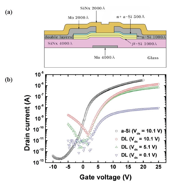
The μc-Si was deposited in a standard 13.56 MHz capacitively coupled RF plasma-enhanced chemical vapor deposition (PECVD) reactor with a SiF4/H2/inert gas mixture, which is known to induce microstructures into the nanocrystalline phases. A-Si was deposited with a SiH4/H2 gas mixture. A 4,000A-thick Mo layer was deposited on glass by sputtering and then patterned for a gate electrode. Four layers of SiNx (4,000 A), a SiF4/SiH4-based DL (lower layer of SiF4[1,000 A] / upper layer of SiH4[1,000 A]), and an n+ a-Si (500 A) layer were deposited on the gate electrode by PECVD. In case of a-Si TFT, a 2,000 A-thick a-Si layer was used instead of a DL layer. A 2,000 A-thick Mo layer was deposited on the n+ a-Si and then patterned for a source/drain electrode. A 2,000 A-thick SiNx passivation layer was deposited on the source/drain electrode. Finally, the DL TFTs were fabri-
cated with W/L = 20/10 μm as shown in Fig.1 (a).
Figure 1(b) shows the typical transfer characteristics of a-Si TFT and DL TFT. The DL TFTs have field effect mobility within 0.5-0.7 cm2/Vs (measured at Vds of 5.1 V), threshold voltages (Vth) within 4-6 V, and subthreshold swings (S.S) within 1.2-1.8 V/decade. The electrical characteristics of the DL TFTs are comparable to those of the conventional a-Si TFTs, except for the offcurrent levels. The abnormality of the off-current level may be caused by several causes, for example, source and drain region conductivity and active layer’s thickness.
To study the DL TFT degradation, various DC bias stresses were applied to the substrates. Specifically, a-Si TFTs were fabricated to compare the degradation differences to DL TFT. The fabrication process of a-Si TFT was identical to that of DL TFT, except that the active layer was replaced with a 2,000 A-thick SiH4-based a-Si layer deposited by PECVD. The degradation mechanisms of a-Si TFTs have already been reported [10-12]. Degradation occurs by charge trapping in the gate insulator and by the creation of dangling bond defects in the channel near the Si-insulator interfaces [10]. Due to these degradation mechanisms, the Vth shift was observed in a-Si TFTs with almost all stress conditions, and the shifts were significantly dominant in the positive gate bias stress.
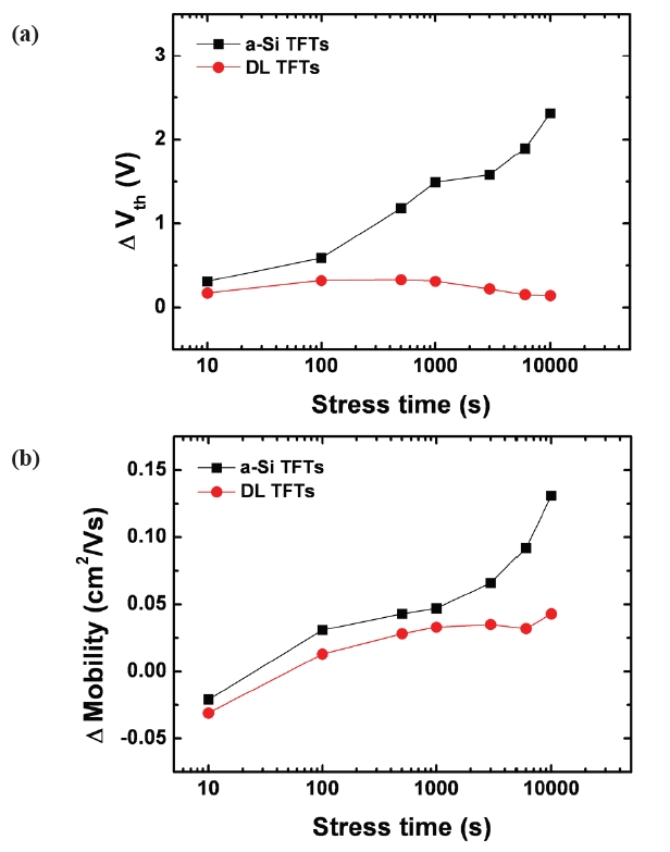
Figure 2 shows the Vth shift and mobility variations of the DL TFT and a-Si TFT after positive gate bias stress (Vgs = 30 V, Vds = 0 V) for 10, 100, 1,000, 3,000, 6,000, and 10,000 seconds.
The DL TFTs do not show the Vth shift degradation phenomenon, while the a-Si TFT suffers a significant Vth shift of approximately 2.4 V. The results of the positive gate bias stress indicate that the degradation mechanism of the DL TFT was not similar to that of a-Si TFT. Although the charge trapping in the SiNx layer and the creation of dangling bond defects in the Si-insulator interfaces are primary factors in the a-Si TFT degradation, in our results, charge trapping in the insulator layer could not be considered dominant because the SiNx deposition conditions were not changed between DL TFT and a-Si TFT. After 10,000 seconds,
the a-Si TFT mobility decrease was measured as 0.13 cm2/Vs, which was approximately two to three times larger than that of DL TFT. The mobility decrease could be attributed to defect generation, such as the breaking of Si-H bonds in the Si channel bulk rather than at the Si-insulator interface.
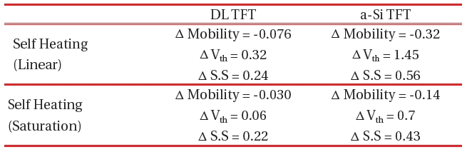
To study the defect generation in the Si channel in more detail, self-heating stress tests were conducted with the DL TFT and a-Si TFT within the linear region (Vgs = 20 V, Vds = 10 V) and saturation region (Vgs = 20 V, Vds = 20 V), respectively. It has been reported that the Vth shift of a-Si TFT in the saturation region could be reduced with respect to the linear region [1]. As Vds increased, the charge injection amount at the Si-insulator interface was lowered,thus reducing the Vth shift degradation in the a-Si TFT. Table 1 shows that the variations in transfer characteristics of the DL TFT and a-Si TFT were measured at Vds = 5.1 V after self-heating stress with (a) Vgs = 20 V, Vds = 10 V, linear region stress and (b) Vgs= 20 V, Vds = 20 V, saturation region stress for 10,000 seconds.
Under the same stress conditions, a-Si TFT had a large Vth shift and polycrystalline Si (poly-Si) TFT had joule heating mobility degradation [13]. In both bias stress conditions of DL TFT, a significant Vth shift was not observed. Additionally, the self-heating degraded DL TFT more in the linear region than in the saturation region, illustrating that the DL TFT has a degradation mechanism similar to a-Si TFT. However, the degradation of DL TFT is much less than that of a-Si TFT under these stresses conditions. On the other hand, in the self-heating operation of poly-Si TFT, degradation was characterized by i) a significant decrease in the on-current value and ii) a significant increase in the off-current value [13]. The research herein revealed that the DL TFT had not suffered the same degradation mechanisms encountered in previous research, suggesting the degradation mechanism was different than that of poly-Si TFT. To this end, the DL TFT was degraded with mechanisms similar to those of a-Si TFT under
the self-heating stress condition. The self-heating degradation was known to be due to the breaking of Si-H bonding in the bulk Si channel rather than at the Si-insulator interface.
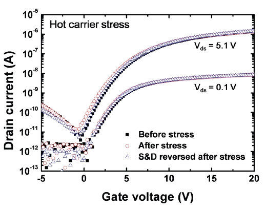
Figure 3 represents the transfer characteristics of the DL TFT measured at Vds = 0.1 V and Vds = 5.1 V before and after the hot carrier stress (Vgs = 5 V, Vds = 20 V, during 10,000 seoncds). After the hot carrier stress, the off- and on-current indicated almost no degradation. The on-current characteristics of the DL TFT were nearly unchanged when measured at low drain voltage (Vds = 0.1 V), indicating the interface states were barely created during hot carrier stress condition.
When the source and drain contacts were reversed after the hot carrier stress, the off-current was slightly lower than the forward measurement. The reduction in current illustrates that the trap states near the drain region of DL TFT are locally created by impact ionization during the bias stress. Similar to DL TFT, the off- and on-current of a-Si TFT had almost no degradation at Vds = 0.1 V and Vds = 5.1 V under hot carrier stress. The similarity under the hot carrier stress may be caused by the similar on-current levels of DL TFT and a-Si TFT, as degradation mainly depends on the applied source-drain voltages, hot carrier concentrations, and material characteristics. The degradation mechanism of poly-Si TFT was caused by the hot carrier stress, with a significant increase of off-current and decrease of on-current [14]. Therefore, in terms of degradation mechanisms, DL TFT was unlike the poly-Si TFT.
In summary, the DL TFTs, which were the same as the conventional a-Si TFTs process except that the active layer was replaced by amorphous/microcrystalline Si DL, were fabricated and the electrical characteristics under DC bias stresses were investigated. The DL TFT is directly applicable to the TFT fabrication process for commercial devices, ensuring efficient fabrication for mass production and is expected to improve the slow deposition rate of the active layer in μc-Si TFT fabrication process, as the deposition rate of a-Si layer is much faster than μc-Si. Because the degradation characteristics of DL TFT were unique, the degradation mechanism of DL TFT is explained unlike that of a-Si TFT or of poly-Si TFT. It is believed that the DL TFT degradation was mainly caused by the defect generation in the Si channel rather than charge trapping in the gate insulator or trap state creation in the region near the drain. It means that the DL TFT could

Variations in transfer characteristics of the DL TFT and a-Si TFT measured at Vds = 5.1 V after self-heating stress with (a) Vgs = 20 V Vds = 10 V linear region stress and (b) Vgs = 20 V Vds = 20 V saturation region stress for 10000 seconds.
achieve higher reliability than a-Si TFT or poly-Si TFT. Therefore, these desirable characteristics of DL TFTs might overcome the limitations of a-Si TFTs and μc-Si TFTs.