Electronic systems combined with semiconductors have recently migrated towards the manufacture of increased density circuits, with the same capability obtainable in a smaller package or increased capability in the same package. This results in a greater susceptibility to various impulses, such as transient overvoltage and electrostatic discharge. Therefore, the electronic devices sensitive to various impulses should be protected by any means.
The zinc oxide (ZnO) varistors are semiconducting solid-state electronic devices formed by sintering zinc oxide with a primary (bismuth, praseodymium, and vanadium) and subordinate additives (cobalt, manganese, chromium, etc). They are switching devices acting with the level of voltage whose resistance decreases drastically when voltage is increased up to the threshold voltage, called varistor voltage. They possess excellent impulse withstanding capability, because ZnO varistors are multi-junction devices that consist of a microstructure of semiconducting ZnO grain-insulating intergranular layer-semiconducting ZnO grain, unlike the zener diode of a single junction. The zinc oxide varistors have been used extensively in the field of circuit overvoltage protection, with applications ranging from a few volts in electronic circuits to millions of volts in electric power systems [1-4].
Most investigations for ZnO-Pr6O11-based varistors have reported on the microstructure and electrical properties in terms of additives and sintering process [3-11]. In particular, Nahm et al. [12-17] reported the effect of rare earth oxides and lanthanum oxide on electrical properties and its stability against direct current (DC) accelerated degradation stress of Zn-Pr-Co-Cr oxides varistors (so-called ZPCC-based varistors). In an application of varistors, one important factor that should be considered in the application is the surge withstand capability. The electronic equipment and the electrical power systems to be protected from various impulses significantly demand a high stability of varistors to enhance reliability. Therefore, the electrical stability against an impulse-current is technologically very important in ZPCC-based varistors [18-23]. These varistor ceramics are limited to 5-components. Therefore, to develop ZPCC-based varistor ceramics for high performance and broad-based applications,it is important to scrutinize the effects of additives and sintering process on varistor properties and degradation behavior against stress. This work addresses the nonlinear electrical properties and impulse degradation behavior of the ZnO-Pr6O11-CoO-Cr2O3-Y2O3-Er2O3 (ZPCCYE) varistors with Y2O3/Er2O3 ratio.
Reagent-grade raw materials were used in the proportions of (98.0-x-y) mol% ZnO, 0.5 mol% Pr6O11, 1.0 mol% CoO, 0.5 mol% Cr2O3, x/y mol% (Y2O3/Er2O3) (x/y = 0.25/0.25, 0.25/0.5, 0.5/0.25, and 0.5/0.5). Raw materials were mixed by ball milling with zirconia balls and acetone in a polypropylene bottle for 24 hours. The mixture was dried at 120℃ for 12 hours and calcined in air at 750℃ for 2 hours. The calcined mixture was pulverized using an agate mortar/pestle and after 2 wt% polyvinyl alcohol binder addition, granulated by sieving through a 100-mesh screen to produce the starting powder. The powder was uniaxially pressed into discs 10 mm in diameter and 2 mm thick at a pressure of 80 MPa. The discs were sintered for 1 hour at 1,350℃ and furnacecooled to room temperature. The heating and cooling rates were 4℃/min. The sintered samples were lapped and polished to 1.0 mm thickness. The final samples were about 8 mm in diameter and 1.0 mm thick. Silver paste was coated on both faces of the samples and the electrodes were formed by heating it at 600℃ for 10 minutes. The electrodes were 5 mm in diameter.
2.2 Microstructure examination
For microstructure characterization, both surfaces of the samples were lapped with SiC paper and polished with 0.3 μm-Al powder to a mirror-like surface. The polished samples were thermally etched at 1,050℃ for 30 minutes. The surface microstructure was examined by a scanning electron microscope (SEM, Hitachi S2400; Hitachi, Tokyo, Japan). The average grain size (d) was determined by the lineal intercept method, given by d = 1.56 L/MN, where L is the random line length on the micrograph, M is the magnification of the micrograph, and N is the number of the grain boundaries intercepted by the lines [24]. The crystalline phases were identified by powder X-ray diffractometer (XRD, Rigaku D/max 2100; Rigaku, Tokyo, Japan) with Ni filtered CuKα radiation. The sintered density (ρ) was measured using a density determination kit (238490) attached to balance (AG 245; Mettler Toledo International Inc., Greifensee, Switzerland).
The electric field-current density (E-J) characteristics were measured using a V-I source (Keithley 237; Keithley Instruments Inc., Cleveland, OH, USA). The breakdown field (E1 mA/cm2) was measured at 1.0 mA/cm2. The nonlinear coefficient (α) is defined by the empirical law, J = C·Eα, where J is the current density, E is the applied electric field, and C is a constant. α was determined in the current density range of 1.0 mA/cm2 to 10 mA/cm2, where α = (logJ2-logJ1)/(logE2-logE1), and E1 and E2 are the electric fields corresponding to E1 = 1.0 mA/cm2 and E2 = 10 mA/cm2, respectively.
2.4 Clamping voltage measurement
The clamping voltage (Vc) was measured at a single pulsecurrent (Ip) of 1, 5, 10, 25, and 50 A with 8 × 20 μs waveform using an impulse generator (Tae-yang Eng., Busan, Korea) and an oscilloscope (TeK 3020B; Tektronix Inc., Beaverton, OR, USA). The pulse-current had a width of 20 μs and a rise time of 8 μs (so-called 8/20 μs wave). The clamp voltage ratio (K = Vc/V1 mA) is

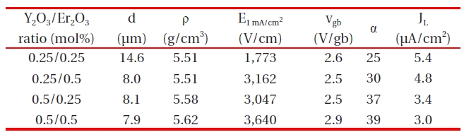
Microstructural and electrical parameters of the samples with different Y2O3/Er2O3 ratios.
defined by the ratio of clamping voltage to breakdown voltage. The breakdown voltage (V1 mA) was measured at a current of 1.0 mA DC.
The impulse-current degradation test was performed at an impulse-current of 400 A using a surge generator. The impulsecurrent had a width of 20 μs and a rise time of 8 μs (so-called 8/20 μs wave). The V-I characteristics were measured at room temperature after applying the impulse-current.
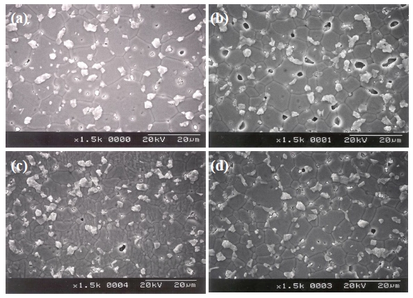
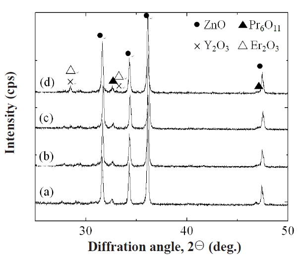
Figure 1 shows SEM micrographs of the samples with different Y2O3/Er2O3 ratios. The average grain size (d) decreased from 14.6 to 7.9 μm with increasing Y2O3 and Er2O3 content. This is attributed to the increase of secondary phases. XRD analysis confirmed that on the surfaces all samples reveal a microstructure consisting of Pr-rich, Y-rich, and Er-rich intergranular layers as a minor secondary phase (whitish), in addition to a major phase of hexagonal ZnO (blackish), as indicated in Fig. .2 The sample added with Y2O3/Er2O3 = 0.5/0.5 generates more intergranular layers. It will be later discussed how the secondary phases will affect degradation behavior against an impulse-current. The sintered density (ρ) increased from 5.51 to 5.62 g/cm3 (theoretical density 5.78 g/cm3 in ZnO) with increasing Y2O3 and Er2O3 content. Table 1 shows the detailed microstructural parameters.
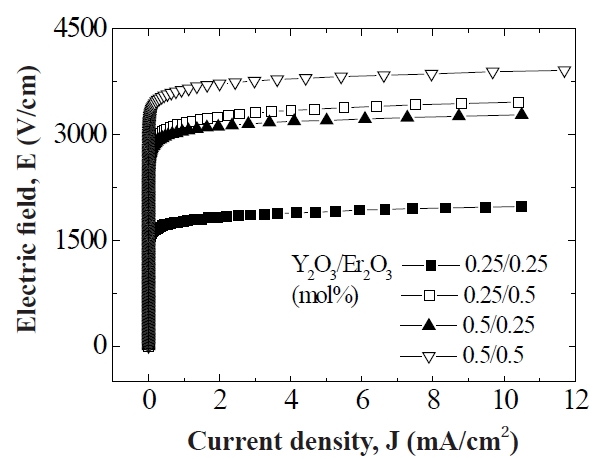
Figure 3 shows the E-J characteristics of the samples with different Y2O3/Er2O3 ratios. It can be seen that the conduction characteristics are divided into a linear region with much higher impedance before the breakdown field and a nonlinear region with much lower impedance after the breakdown field. The E-J characteristic parameters calculated from Fig. 3 are shown in
[Table 2.] Clamping voltage and clamp voltage ratio of the samples with different Y2O3/Er2O3 ratios.
Clamping voltage and clamp voltage ratio of the samples with different Y2O3/Er2O3 ratios.
Table .1 The breakdown field (E1 mA/cm2) increased with increasing Y2O3 content for the fixed Er2O3 content and with increasing Er2O3 content for the fixed Y2O3 content. The increase of E1 mA/cm2 can be explained by the increase in the number of grain boundaries due to the decrease of average ZnO grain size as follows: E1 mA/cm2 = vgb/d, where vgb is the breakdown voltage per grain boundary, and d is the average grain size. The sample added with Y2O3/Er2O3 = 0.5/0.5 exhibited the maximum value (3,640 V/cm)and the minimum value (1,773 V/cm) in the E1 mA/cm2· The vgb values with different Y2O3/Er2O3 ratios were within the normal range of values of 2-3 V/gb. The nonlinear coefficient (α) increased with increasing Y2O3 content for the fixed Er2O3 content and with increasing Er2O3 content for the fixed Y2O3 content. Thus, the
samples added with Y2O3/Er2O3 = 0.5/0.5 exhibited the maximum value (39) of α and the samples added with Y2O3/Er2O3 = 0.25/0.25 exhibited the minimum value (25) of α. The increase of α value with increasing Y2O3 and Er2O3 content may be attributed to the lowering of the Schottky barrier, because of the variation of the electronic state at the grain boundaries. The variation of JL shows an inverse relationship to the variation of α with different Y2O3/Er2O3 ratios. Thus, it can be seen that the values of α and JL were significantly affected by the Y2O3/Er2O3 ratio.
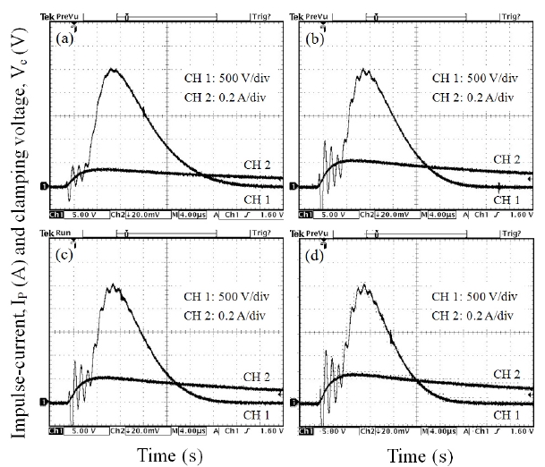
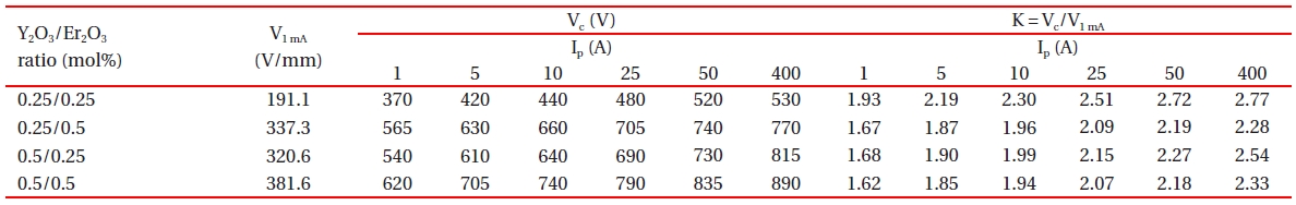
Figure 4 shows the clamping voltage (Vc) corresponding to an impulse-current of 1 A of the samples with different Y2O3/Er2O3 ratios. The Vc is defined by the drop voltage between electrodes of the sample when the specified impulse-current flows through the sample [18,19]. The higher impulse-current leads to the higher Vc, because the resistance in the nonlinear region exists still as a low value [18-23]. Table 2 summarizes the clamping voltage (Vc) and clamp voltage ratio (K) corresponding to the lower impulsecurrent of 1-50 A of the samples. The samples added with Y2O3/Er2O3 = 0.25/0.25 exhibited the highest clamp voltage ratio (K) of K = 1.93-2.72. That is, this composition ratio shows the worst clamping behavior. On the contrary, the samples added with Y2O3/Er2O3 = 0.5/0.5 exhibited the lowest clamp voltage ratio (K) of K = 1.62-2.18. That is, this composition ratio shows the best clamping behavior. In addition, the samples added with Y2O3/Er2O3 = 0.25/0.5 showed good clamping behavior with clamp voltage ratio (K) of K = 1.67-2.19 comparable to the samples added with Y2O3/Er2O3 = 0.5/0.5. These experimental facts show that the Y2O3/Er2O3 ratio has a significant effect on the impulse characteristics. Furthermore, it can be seen that the higher breakdown voltage leads to the higher clamping voltage and the lower K value. The low K value means that the varistor better clamps an

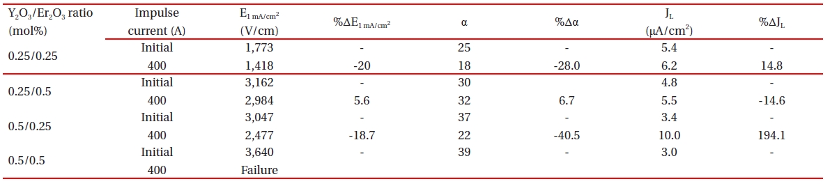
E-J characteristic parameters before and after applying the impulse-current of the samples with different Y2O3/Er2O3 ratios.
impulse-current to operating voltage.
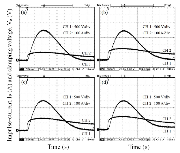
Figure 5 shows the applied impulse-current and clamping voltage waves to investigate degradation behavior against an impulse-current of 400 A with different Y2O3/Er2O3 ratios. The samples added with Y2O3/Er2O3 = 0.25/0.5 exhibited the best clamping characteristics, with voltage ratio (K) of K = 2.28, as shown in Table 2.
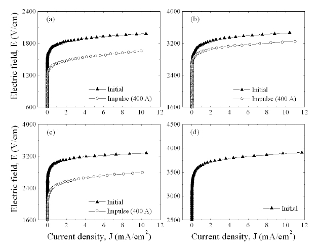
Figure 6 compares the variation of E-J characteristics after applying the impulse-current of 400 A with the initial E-J characteristics with different Y2O3/Er2O3 ratios. It can be seen that the E-J characteristic curves shifted toward a low field region(downward in Fig.6 ) in the breakdown region after applying the impulse-current. This is entirely different to the characteristic E-J behavior, which shifted toward a high current region (rightward)in the prebreakdown region after applying the DC accelerated degradation stress [15]. The samples added with Y2O3/Er2O3 =0.25/0.25 exhibited the smallest variation of E-J characteristics in the nonlinear region after applying the impulse-current. On the contrary, the samples added with Y2O3/Er2O3 = 0.5/0.5 destroyed at an impulse-current of 400 A. This sample possesses many secondary phases at the grain boundaries and triple points. This will result in the decrease of effective area of the grain boundary [15]. Thus, this failure against an impulse-current is attributed to very high current impulse density per grain boundary due to many secondary phases.
Table 3 summarizes the variations of the breakdown field (%ΔE1 mA/cm2) and the nonlinear coefficient (%Δα) after applying the impulse-current of 400 A. The samples added with Y2O3/Er2O3
= 0.25/0.5 exhibited the lowest %ΔE1 mA/cm2 = -5.6% after applying the impulse-current of 400 A. The samples added with Y2O3/Er2O3= 0.25/0.25 exhibited the highest %ΔE1 mA/cm2 = -20.0% after applying the impulse-current of 400 A. Thus, the samples added with Y2O3/Er2O3 = 0.25/0.5 show very good stable E1 mA/cm2 characteristics against an impulse-current, as recording the variation rate much less than 10% as a specification in commercial varistors. The %Δα after applying the impulse-current of 400 A was only 6.7% for the samples added with Y2O3/Er2O3 = 0.25/0.5, whereas the remainder exhibited the %Δα >20%.
The nonlinear electrical properties and degradation behavior against an impulse-current of 400 A in the ZnO-Pr6O11-CoOCr2O3-Y2O3-Er2O3 (ZPCCYE) varistors were investigated with the Y2O3/Er2O3 mole ratio. The Y2O3/Er2O3 ratio has a significant effect on nonlinear electrical properties and impulse degradation behavior of the ZPCCYE varistors. The breakdown field (E1 mA/cm2) and nonlinear coefficient (α) increased with increasing Y2O3 and Er2O3 content. The varistors added with Y2O3/Er2O3 = 0.5/0.5 exhibited the best nonlinear properties with 39 in nonlinear coefficient and the best clamp characteristics, in which the clamping voltage ratio (K) was in the range of K = 1.62-2.18 at an impulsecurrent of 1-50 A. The varistors added with Y2O3/Er2O3 = 0.25/0.5 exhibited the best electrical stability, with %ΔE1 mA/cm2= -5.6%, %Δα = 6.7%, and %ΔJL = -14.6% against an impulse-current of 400 A. On the contrary, the varistors added with Y2O3/Er2O3 = 0.5/0.5 were destroyed by applying an impulse-current of 400 A.