The determination of the fabricated design area in research and development of solar cells for high-efficiency power conversion is very important. There is a direct relationship between the design area and charge density in the
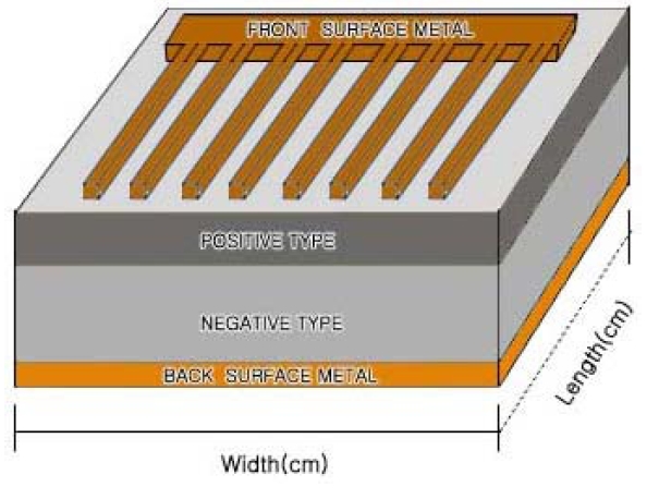
Therefore, this design technology involves a set of technologies to increase power-conversion efficiency by increasing electron density. A typical device structure which is routinely used for high-efficiency device fabrication consists of a
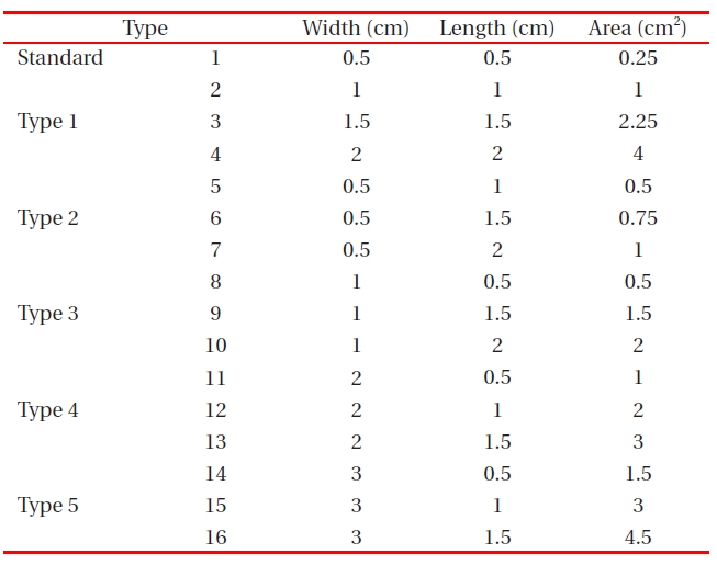
The following sequence of processing steps is generally used for device fabrication. This paper investigates the changes in charge density with various solar-cell fabrication design areas (width [cm] × length [cm]) for standard, type 1, type 2, type 3, type 4, and type 5 designs. In addition, the effects of chargedensity changes and current output were investigated as direct effects. The charge density is the total amount of charge in a fixed length or area divided by the material volume [1].
The electrical properties of semiconductors related to doping and to states which exist deep in the band gap can be conveniently measured using the depletion capacitance of a diode.
The present treatment of
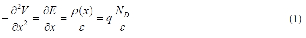
where ε is the dielectric constant and

and that for the electrostatic potential is:

where V

where Vbi is the “built-in” potential and V is the applied bias. For one-sided and abrupt junctions, the depletion depth is given by:

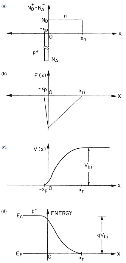
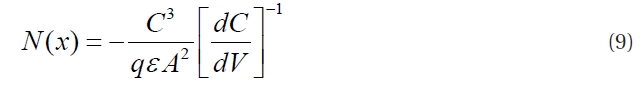
The solution for the electrostatic potential is often drawn superimposed on the band structure as shown in Fig.2 (d) as a “band-bending diagram.” Here, the Fermi level does not vary across the junction if no bias is applied because the Fermi level is the chemical potential of the carriers, which must be constant in equilibrium. The crossing point between the Fermi level and the donor level determines the depletion depth. If a slight bias, ΔV, is applied, then according to Eq. 6,
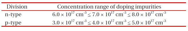
[Table 1.] Concentration range of doping impurities for calculations.

Concentration range of doping impurities for calculations.
[Table 2.] Experimental design for solar-cell charge-density analysis in the depletion region.
Experimental design for solar-cell charge-density analysis in the depletion region.
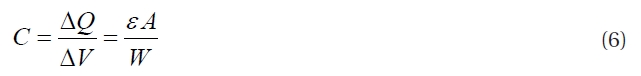
This is a basic result which is easy to remember because it is identical to that for a parallel-plate capacitor. If there is a quiescent applied bias, V, which increases the depletion depth (i.e., the reverse bias), then the capacitance is decreased, and this affords a convenient way to ascertain the polarity of a diode. It follows from Eqs. (4) and (6) that:
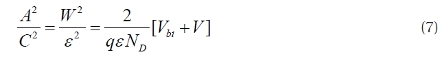
This key result implies that by plotting
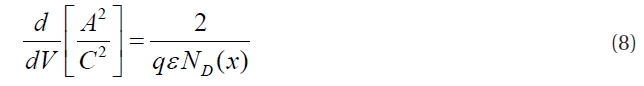
which is often stated as:
where
[Table 3.] Multipliers for various solar-cell areas according to the experimental design.
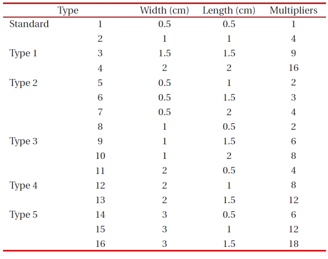
Multipliers for various solar-cell areas according to the experimental design.
where
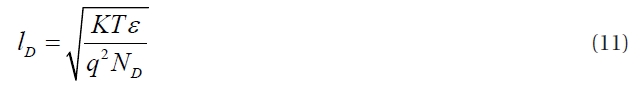
K is Boltzmann’s constant, and T is the temperature.
3. CALCULATION PARAMETERS FOR THE DERIVATION OF THE INTERNAL ELECTRIC FILED
The impurity doping concentrations for a
The doping impurity concentrations in solar-cell fabrication are determined by the different electrical properties in the two kinds of surface material. For
Table 2 shows an experimental design for solar-cell chargedensity calculations.
The design multiplier for different solar-cell areas of standard, type 1, type 2, type 3, type 4, and type 5 designs are shown in Table .3The solar-cell area is calculated as width (cm) × length (cm). The solar-cell area is directly related to the short circuit current (A). However, the relation between power-conversion efficiency (η) and area is not a direct relationship.
In this section, the results obtained on the basis of the chargedensity fabrication experimental design will be discussed. The discovery of the
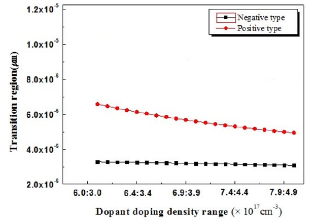
tions. Both types of transition parameter depend on the impurity doping concentration. However, fabricated solar-cell area is unrelated to charge density over most of the depletion region.
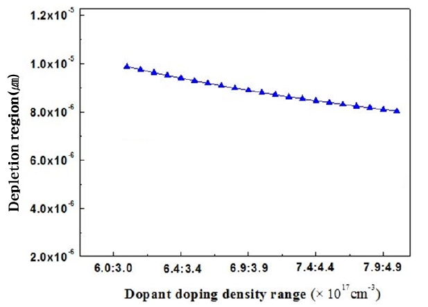
The depletion parameter for the normal range of standard impurity doping concentrations was calculated as 8.0 × 10⁻⁶ μm. In addition, the
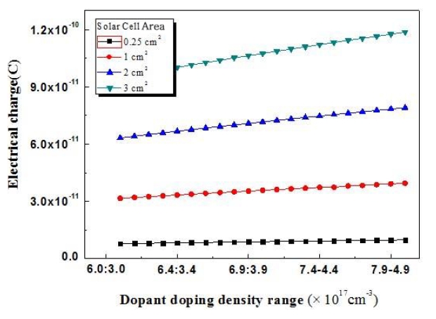
includes both positive and negative ions. The minimum dopant impurity concentrations were 6.0 × 1017 cm-3 and 3.0 × 1017 cm-3 for Si2H6 and DEZn respectively. The maximum impurity doping concentrations were 8.0 × 1017 cm-3 and 5.0 × 1017 cm-3 for Si2H6 and DEZn respectively. Figure 5 shows the variation of the
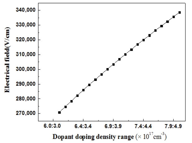
tion region and depends on impurity doping concentrations of both negative and positive types. The transition region is determined by the ionization carrier and by changes in the Fermi level due to variations in impurity doping concentrations.
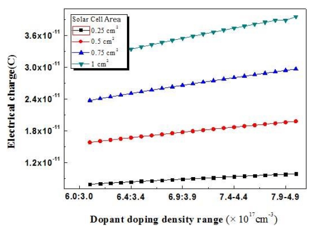
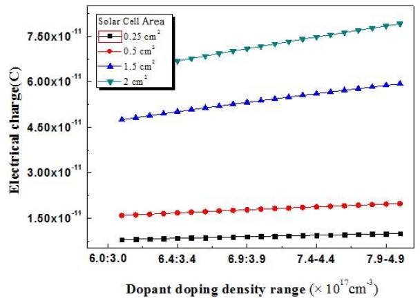
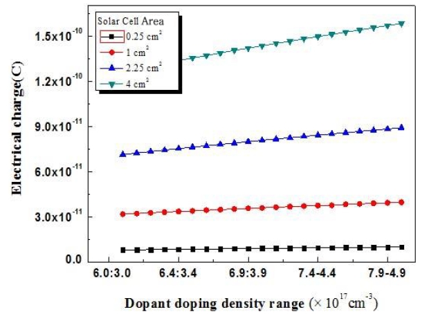
The electric field created by the space charge region opposes the diffusion process for both electrons and holes. Figures 6-10 show changes in charge density which reflect the results obtained for the fabricated solar cells.
The fabricated solar-cell experimental design was implemented for standard, type 1, type 2, type 3, type 4, and type 5 solar cells. The charge density was found to be very high for the solar cell of 4.5 cm2 area. In addition, the charge density was found to increase with increasing solar-cell area. The carrier density was determined with silicon and GaAs material.
So far, this discussion has considered the basic p-n junction structure. The average length that an electron travels through the p-type material before recombining is called the diffusion length and is typically on the order of microns [4]. The built-in potential barrier maintains an equilibrium between the majority carrier electrons in the
In conclusion, this research has examined variations in the charge density according to a solar-cell fabrication experimental
design. The current was found to vary as a function of the charge density and the solar-cell area. The Fermi level was also affected by the impurity doping concentration; in the depletion region, the relationship was direct. The ionization carrier is a space of continuous motion in the osmosis interface between the two kinds of semiconductors. A mathematical foundation was also presented in this paper for the analysis of charge-density variations as a function of solar-cell area.