Thin films of multiferroic materials, which exhibit simultaneously ferroelectric, ferromagnetic, antiferromagnetic, and ferroelastic behaviors, have become a renewed focus of attention recently because of their potential application in micro- and integrated electronic or spintronic devices. Various deposition methods, including the sol-gel method, metal-organic solution deposition, RF sputtering, and pulsed laser deposition, were used to prepare heteroepitaxial or polycrystalline multiferroic thin films [1-3]. However, most multiferroic materials are not promising for device applications because their transition temperatures for ferroelectricity or magnetic ordering are lower than room temperature. On the other hand, among the many multiferroic materials, bismuth ferrite (BiFeO3, BFO) attracts much attention because it is G-type antimagnetic below the Neel temperature of 370℃ and ferroelectric below the Curie temperature of 850℃, and therefore the magnetoelectric effect can be expected to occur even at room temperature [4]. BFO is attractive as a ferroelectric material for high-density ferroelectric random access memories because of its large remnant polarization. However, BFO has serious problems as a ferroelectric material because it has a rather large leakage-current density, especially at room temperature. As a result, dielectric breakdown occurs easily even at low field strengths, thereby creating difficulties in pulling film. Moreover, the highly electrically conductive nature of BFO makes it difficult to obtain excellent ferroelectric properties. To overcome this problem, various approaches have been proposed, including a substitution technique using Mn and Ti at
the B-site, La and Nd at the A-site [5,6], or both, and the formation of a solid solution with Pb(Zr,Ti)O3 and BaTiO3 [7,8]. There are many reports of a reduction in the leakage current induced by doping and formation of a solid solution. In these investigations, a metal-insulator-metal capacitor structure is used for current measurement. Note that the current measured in the capacitor structure includes contributions from the grain boundaries or microstructure of the films. The authors have already reported on the good dielectric properties, especially high remnant polarization and low leakage current densities, of lead zirconate titanate (PZT) heterolayered thin films alternately spin-coated using PZT(20/80) and PZT(80/20) metal alkoxide solutions [9]. In this study, BFO/PZT multilayer thin films were prepared by the sol-gel method and then were spin-coated onto a platinized Si substrate alternately using BFO and PZT metal alkoxide solutions. The objective of the present study is to investigate the fabrication and electrical properties of PZT/BFO multilayer thin films for electronic memory device applications. The study also intends to investigate the role of the lower film in crystallization of the upper film during annealing and the electrical properties of PZT/BFO multilayer thin films for electronic memory device applications.
BiFeO3 and Pb(Zr0.52Ti0.48)O3 with excess Pb-acetate 10 mol% precursor solutions were prepared by the sol-gel method from Bi-nitrate pentahydrate [Bi(NO3)3·5H2O], Fe-nitrate nonahydrate [Fe(NO3)3·9H2O], Pb-acetate trihydrate [Pb(CH3CO2)2·3H2O], Zr
BFO/PZT films as the top electrode with a diameter of 250 μm.
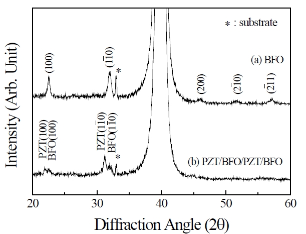
Figures 1(a) and (b) show XRD patterns of BFO single film and four-layer PZT/BFO (PZT/BFO/PZT/BFO) film respectively. Figure 1(a) shows the typical XRD pattern of a rhombohedral structure, and a second phase such as Bi2Fe4O3 or a preferred orientation were not observed. However, the XRD pattern of the BFO thin film coated on the PZT layer depicted in Fig.1 (b) reveals that peak splits of (100)/(001) and (101)/(110) at 2θ = 21° and 32° occurred and were shifted to the lower-angle side. This property can be understood in terms of the effect of the lower layer. More-
over, it can be assumed that the crystal growth of the upper BFO layer can be influenced by the lower PZT layer and that the crystallization behavior of the resulting film has been controlled by the choice of the initial or seed layer.
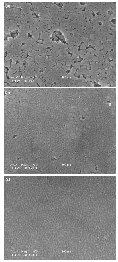
Figures 2(a-c) show surface field emission scanning electron microscope micrographs of PZT, three-layer PZT/BFO/PZT, and five-layer PZT/BFO/PZT/BFO/PZT thin films respectively. The thickness of the film after one cycle of drying and sintering was approximately 70-80 nm. The PZT single film (Fig.2 (a)) shows a uniform grain structure with an average grain size of 30-40 nm. Many pores were also observed in the film. However, the threelayer and five-layer PZT/BFO multilayer thin films (Figs. 2(b) and(c)) show a uniform and void-free grain structure and a grain size smaller than that of PZT single film. The reason for this is assumed to be that the lower BFO layers play an important role as a nucleation site or seed layer for the formation of homogeneous and uniform upper PZT layers.
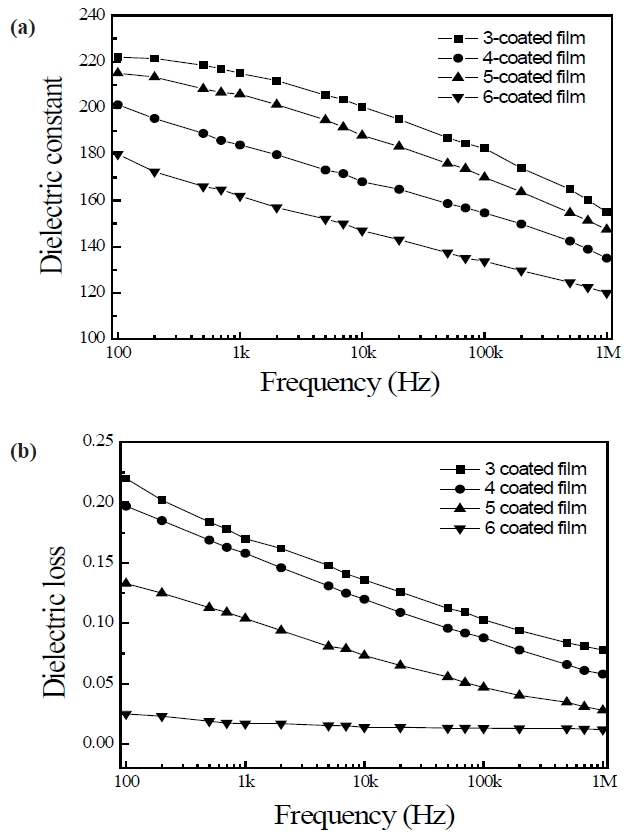
Figure 3 shows the variations in the relative dielectric constant and the dielectric losses of PZT/BFO thin films as a function of frequency at 25℃. The relative dielectric constant decreased with an increase in the applied frequency, and the PZT/BFO multilayer thin films exhibited typical frequency-dispersion behavior. The dielectric constant and dielectric losses decreased with an increase in the number of layers, and the six-layer PZT/BFO thin film exhibited good values for these properties, 162 and 0.017 at 1 kHz respectively. This phenomenon can probably be explained by the fact that the diffusion of Pb from the PZT film into the Pt bottom electrode and the diffusion of Pb, Ti, Zr, Bi, and Fe at the interfaces between the PZT film and the BFO film is intensified with an increase in the number of layers, or in other words, an increase in the number of annealing processes [10]. Interfacial layers with low dielectric constant are formed at the interfaces between BFO and PZT layers. The dielectric constants of three-
and five-layer PZT/BFO thin films with a top layer of PZT(52/48) were larger than those of four- and six-layer PZT/BFO thin films with a top layer of BFO. The reason for this is assumed to be that the volatilization temperature of Pb (886℃) is higher than that of Bi (825℃). The three- and five-layer PZT/BFO thin films have a more stoichiometric composition. Dielectric losses decreased with an increase in the number of layers because the interfaces between PZT and BFO layers act as sinks for the charges. However, further investigation and discussion are necessary to understand the dielectric properties of PZT/BFO multilayer films.
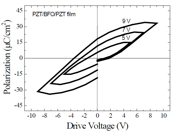
Figure 4 shows the polarization-electric field (P-E) hysteresis loops of the three-layer PZT/BFO (PZT/BFO/PZT) multilayer thin film. The centers of the hysteresis loops are not located at zero bias voltage, but are shifted toward negative bias voltage. It is suggested that an internal bias field has been induced at the interface between the lower electrode and the PZT films by the difference in thermal history between the upper and lower electrodes.
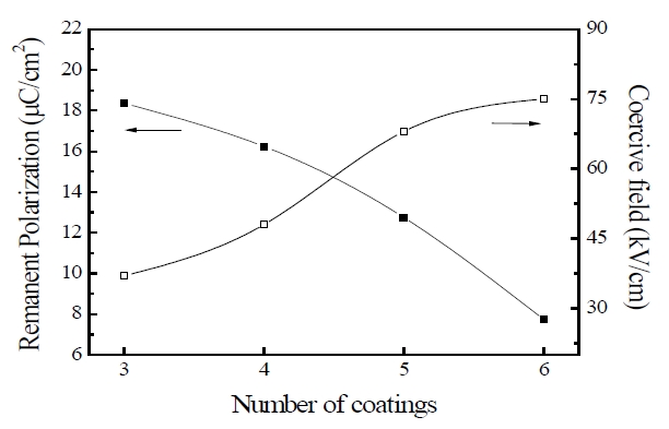
Figure 5 shows the variation in the remnant polarization and the coercive field of the PZT/BFO thin films with the number of layers. The remnant polarization decreased and the coercive field increased with an increase in the number of layers. These properties may be understood in terms of increasing the formation of a second phase with low permittivity at the interfaces between layers and of sinks that trap charges forming at interfaces. These second phases act as sinks for charges and inhibit their spatial movement. As a result, the coercive field increased with increasing number of layers. The remnant polarization and the coercive field of the PZT/BFO/PZT thin films were 18.36 μC/cm2 and 37 kV/cm respectively.
In this paper, Pb(Zr0.52Ti0.48)O3 and BiFeO3 alkoxide solutions were prepared by the sol-gel method, and PZT/BFO multilayer thin films were spin-coated onto a Pt/Ti/SiO2/Si substrate alternately using PZT(52/48) and BFO alkoxide solutions. Threeand five-layer PZT/BFO multilayer thin films showed a uniform and void-free grain structure, and the grain size decreased with increasing number of layers. The reason for this is assumed to be that the lower layers play an important role as a nucleation site or seed layer for the formation of homogeneous and uniform upper layers. The remnant polarization and dielectric losses decreased and the coercive field increased with an increase in the number of coatings. These properties may be understood in terms of the formation of interfaces between PZT and BFO layers which act as sinks for the charges. More investigation and discussion are required to understand the charge distribution characteristics at the interfaces of PZT/BFO multilayer films.