The problem of the short channel effect is becoming serious,because the gate length of the metal oxide semiconductor field effect transistor is shrinking to less than 45 nm. This device has many advantages, including high drive current, high conductance,ideal sub-threshold slope. Therefore, many researchers have studied new structure and material to overcome these problems. Titanium nitride (TiN) was studied as attractive material due to its many advantages, such as TiN thin film having characteristics of low resistivity, low diffusion coefficient, chemical stability, good hardness, and high compatibility with high-
This metal layer is between a poly-Si layer and a dielectric layer. The dielectric layer generally consists of SiO2 or high-k material. Damage of these layers is inevitable during the etching of the TiN metal layers. Notching and lateral etching of the poly-Si and metal layers can cause short channel effects by unintended infiltration of species into the active channel. Therefore,we needed to further consider the roles of noble gas in the dry etching process. Noble gas enhances the volatility of the etch byproducts by ion bombardment of the sample during the etching process. However, each noble gas produces a different effect during the etching process due to their different physical characteristics [9,10].
In this study, we investigated the etching characteristics of TiN thin film using an inductively coupled plasma (ICP) system. The chemical reactions on the surfaces of the etched TiN thin film were investigated using X-ray photoelectron spectroscopy (XPS).
13.56 MHz asymmetric RF generator to control the direct current(DC)-bias voltage. The distance between the quartz window and substrate electrode was 9 cm. The chamber was evacuated to 10-6 torr using a mechanical pump and a turbo molecular pump. The process conditions were as follows; RF power 500 W, DC-bias voltage -100 V, process pressure 15 mTorr, and substrate temperature 40℃. The TiN thin films were etched in BCl3/Ar plasma.The etch rates were measured using a depth profiler (Alpha-Step 500; KLA Tencor, San Jose, CA, USA). The chemical reactions on the surfaces of the etched TiN thin films were evaluated using XPS (Thermo VG, SIGMA PROBE; East Grinstead, West Sussex,England). The source type for the XPS analysis was Al Kα with a spot size of 400 ㎛. The energy step size was 0.1 eV.
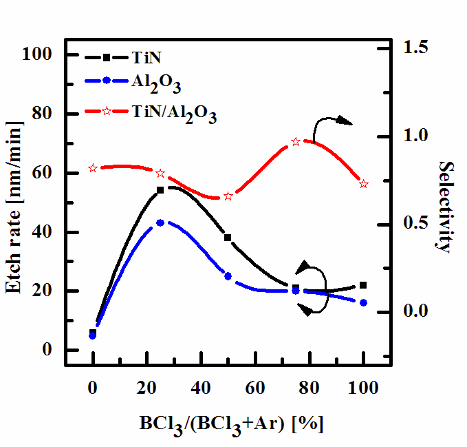
Plasma etching of TiN thin film and Al2O3 thin film were systematically investigated, as a function of the BCl3/Ar gas mixing ratio, to characterize TiN thin film in an ICP system. Figure 1 shows that the etch rate of TiN thin film and Al2O3, as a function of BCl3/Ar plasma gas mixing ratio, when total flow rate was maintained at 20 sccm. Other process conditions, such as RF power, DC-bias voltage, and process pressure were also maintained at 500 W, -100 V, and 15 mTorr, respectively. As the BCl3/Ar gas mixing ratio increases, the etch rates of TiN thin film and Al2O3 thin film decreases. The maximum etch rates of TiN thin film and Al2O3 thin film are 54 nm/min, 43 nm/min at a BCl3/(BCl3+Ar) of 25% and increased with further addition of BCl3 gas.
This allows one to assume that, for a given range of experimental conditions, a physical etch pathway is more effective than a chemical one. In our opinion, the domination of physical etch pathway may be explained by two reasons. First, the melting point (M.P.) for TiN thin film is about 3,290℃, so that it can be related to hardly volatile compounds. Second, the strength of the Ti-Cl4 chemical bond (M.P.: -24℃) is lower than one for Ti-N. Therefore, Cl atoms formed in plasma can react with TiN thin film spontaneously and ion bombardment is needed to support physical reaction by breaking chemical bonds. One can propose at least three mechanisms to explain the non-monotonic behavior of the TiN etch rate: 1) non-monotonic changes of both
volume densities and fluxes of active species resulted from the influence of plasma parameters on volume kinetics; 2) a concurrence of two etching mechanisms with monotonic, but opposite tendencies to change with decreasing BCl3 mixing ratio (for example,decreasing flux of chemically active species and increasing efficiency of ion stimulated desorption of reaction products due to increasing flux of Ar+ ions). It was shown that variation of gas mixing ratio causes monotonic changes of electron density,electron temperature, ion density, and Cl atom density. Accordingly,we can assume the same monotonic behaviors for fluxes of these species and, in fact, the first mechanism among ones proposed above can be neglected. In our opinion, the second and third mechanisms work simultaneously [11].
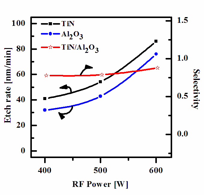
Figure 2 shows the etch rate of TiN thin film and Al2O3 thin film, as a function of RF power. Other process conditions, such as a BCl3 (25%)/Ar (75%) plasma, DC-bias voltage, and process pressure were also maintained at -100 V, and 15 mTorr. As RF
power increases, the TiN thin film and Al2O3 thin film also increases,starting from 41 nm/min and 32 nm/min at 400 W, but reaches a maximum of 86 nm/min and 76 nm/min at 600 W. An increase in RF power causes a monotonic increase in both dissociation and ionization rates and thus, in densities and fluxes of Cl atoms and positive ions. In our case, such a layer can result from the deposition of solid Cl that then is bonded with surface oxygen to form Ti-Cl, as well as from Cl radicals incorporated in the polymer-like structure.
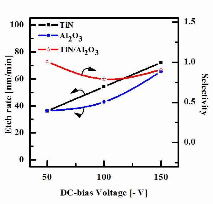
Figure 3 shows the etch rates of TiN thin film and Al2O3 thin film, as functions of DC-bias voltage. Other process conditions,such as a BCl3 (25%)/Ar (75%) plasma, the RF power and the process pressure were also maintained at 500 W, and 15 mTorr.As the DC-bias voltage increases from 50 to 150 V, the etch rate of TiN thin film and Al2O3 thin film increases from 36.2 to 72.1 nm/min and from 36.4 to 65.4 nm/min. The selectivity of TiN to Al2O3 slightly decreased. An increase in etch rate can be related to the increase of mean ion energy, resulting in increasing sputtering yields for the TiN thin film, Al2O3 thin film and reaction products[12].
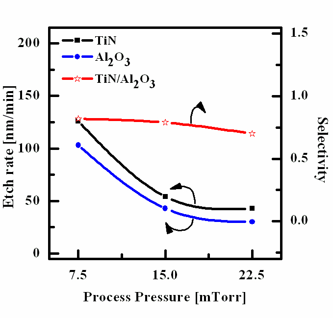
Figure 4 shows the etch rates of TiN thin film and Al2O3 thin film as a function of process pressure. In our opinion, the situation regarding the effect of process pressure is as follows. Other process conditions, such as, BCl3 (25%)/Ar (75%) plasma, RF power and DC-bias voltage were maintained at 500 W, and -100 V. An increase in process pressure decreases the density of neutral chemically active species, but higher ion mean free path and ion energy. Thus, with increasing process pressure, we have a tendency to accelerate in the physical etch pathway, but a worse condition for ion stimulated desorption of reaction products probably results in decreasing the fraction of free surface acceptable for chemical reaction. Similarly to the effect of gas mixing ratio, these two factors, working in opposite direction, produce a non-monotonic behavior of the etch rate [12].
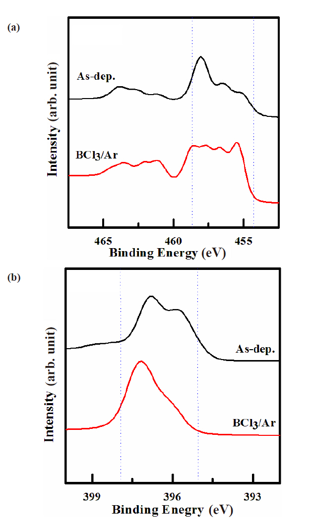
XPS analysis was used to investigate chemical states of the etched surfaces of the TiN thin films. Figure 5 shows narrow scan spectra for Ti 2p and N 1s from TiN thin film surfaces. Figure 5(a) shows that the Ti 2p spectra were at a binding energy of 458 eV, suggesting that Ti remained fully nitride after etching. These spectra intensity on the as-deposition and BCl3/Ar plasma were closely similar due to volatile etching by-product. As the BCl3 content in the BCl3 /Ar plasma increases, the intensity of this
peak also decreases [10,13-16]. Therefore, this conclusion is in good agreement with the data of Fig. 1 Figure 5(b) shows the intensities of 396.8 eV peak reversed for the data obtained from the as-deposited and etched samples. That is, the shoulder peak,indicated from the as-deposited sample related to the formation of N-Ti bonds, decreased significantly due to the preferential removal of the Ti atoms. With the addition of BCl3 gas, the Ti-N peak intensity became negligible, which demonstrates a dramatic increased chlorination of the etched surface. The intensities of the N-Ti peaks decreased presumably due to the increased formation of TiClx in the air. There is also the possibility of Ti-N bond formation, even though that was not demonstrated here[11,12,17].
In this study, we studied the etching characteristics of TiN thin films as functions of Ar additive to BCl3 plasma and the DC-bias voltages. TiN thin films were etched by each additive noble gas to BCl3 plasma. The higher etch rate of the TiN thin films was at BCl3 (25%)/Ar (75%) plasma. This can be explained by Ar affecting physical effects on the surface during the etching process.The chemical reactions on the surface of the etched TiN thin film were explained using XPS analysis. The reason for etch rate maximum is the concurrence of physical and chemical pathways in ion-assisted physical reaction. It was suggested that nonvolatile oxygen compounds, such as the XPS result, showed that the composition of the etched sampled in the BCl3 plasma is identical to that of the as-deposited sample. This tendency was very similar to the etch characteristics. This result agreed with the general energy dependency of ion enhanced chemical etching yields.