Polymeric films coated with thin metallic film have been extensively used as flexible printed circuit board (FPCB) and electromagnetic shielding materials [1-3]. Physical and chemical properties of polymers differ depending on the type of polymer used [4]. Therefore, an appropriate polymer should be selected based on the required characteristics. The plating material also has to be chosen according to the properties required. The properties of metals differ from those of polymers, thus grafting the two to create a single composite confers the usefulness and the advantages of both metals and polymers to the composite material.However, we need a grafting method and process, because it is not easy to integrate the two. In general, the surface of polymer has to be etched or modified prior to the plating to have holes or ditches that anchor the plated metal with good adhesion to the surface of polymer [5].
Usually wet etching processes have been used with chemicals such as dichromic acid, fluoridation-hydrogen acid, and hydrochloric acid to give the anchoring sites to a polymer [6].These processes have caused environmental problems. The wet etching processes differ from polymer to polymer [5]. Others techniques to alter the surface of polymer physically and/or chemically that are environment-friendly include glow discharge, plasma irradiation in a vacuum chamber and ultrasound treatment [7]. However, none of the above methods so far proved to be effective for use in industry due to their low productivity and high cost of maintenance compared to conventional processes.
Polypropylene (PP) is a widely used polymeric material for parts of electric and electronic devices and for automobile parts,because it can be processed easily and has high thermal resistance,high mechanical strength, and high chemical stability against bases, acids, and moisture [4]. The surface of PP can be hardly chemically etched compared to those of other polymers,such as acrylonitrile-butadiene-styrene, for the electroless plating,due to its high chemical stability. Thus PP films covered by thin metallic film with high strength of adhesion between them would be useful as a composite material.
In this study, we have introduced the plasma induced surface modification method as an environmentally friendly process for the pre-treatment of the surfaces of PP films prior to the electroless plating. This can be processed in air at atmospheric pressure with dielectric barrier discharges (DBDs). The morphological changes of the samples were observed using scanning electron microscope (SEM) and the wettability of the sample surface was deduced from the static contact angle measurement to understand the adhesion mechanism of the coated metallic film on PP film, before and after plasma treatment. The cross-sectional images were taken by SEM to see how well the plating is fused into the surface of PP film. The adhesion strength of the metallic films on the PP films was examined by the thermal shock test and the cross-cutting and peel test. We have found a method to produce a composite material of nickel (Ni) and PP films with high quality.
Commercially available PP films about 100 mm × 50 mm and 0.5 mm thick were prepared for surface modification induced by atmospheric plasma treatment and for electroless plating.
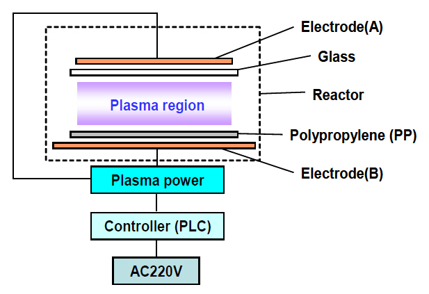
The system for the surface modification of PP films consists of a power supply for plasma generation, a controller to switch on and off the power supply according to the instruction sequences that can be implemented into the controller via computer interface,and a reactor in which plasma is produced and the surface modification occurs. There is no matching box between the power supply and the reactor. Only air is used as a plasma generating gas. The whole system for plasma was operated in open space at room temperature. The power supply, which is homemade, provides a high voltage alternating current output with a maximum peak voltage of 15 kV, maximum effective current of 100 mA, and frequency of 20 kHz. DBDs [8] were employed for uniform and stable plasma formation over all areas of the PP film surface at atmospheric pressure. A common glass sheet 2 mm thick was used for the dielectric barrier, copper plates 2 mm thick for highly thermal conductive electrodes. Figure 1 shows schematically a configuration of the electrodes and the dielectric barrier. The controller is composed of solid state relays and a programmable logic controller. The temperature of the reactor was monitored using an infrared thermometer during the process of PP film surface modification.
Ni was chosen as the metal to be coated on PP films, because it was the only metal that could be grafted by the electroless plating in our lab.
2.2 Sample preparation and surface modification by DBDs
PP films were first washed out with tap water, and then sonicated in a water bath for a couple of minutes to remove physical adsorbates. In general, the release agent remains on the surface of polymeric products. Thus, there must be a process of removal of the release agent using surfactant solutions to have good plating in the electroless plating process. However, we did not remove the release agent, because it was supposed to be removed during the surface modification process by plasma.
Dried samples were placed over the lower electrode of the reactor, as in Fig. 1.The samples were installed inside the reactor,such that only the top sides were processed by plasma; the bottom sides were so tightly close to the bottom electrode not to be processed by plasma. The sample size (100 mm × 50 mm) was made sufficiently small, due to the difference in plasma density between on the edge region and on the central region of the reactor, so that the entire range of the sample surface could be plasma treated evenly.
The reactor was placed in open space at room temperature during the surface modification process and operated at atmospheric pressure with air. 70 W power was supplied for plasma generation.
Plasma treatment of the polymer over a long successive period could result in physically and chemically irrecoverable damage to the polymer. Thus in this study, the continuous processing time and the idle time were determined by preliminary experiments to ensure only the surface of PP film is modified physically and/or chemically. Then, the controller was programmed to generate plasma on the PP film surfaces with the total plasma treatment times, 10 seconds, 20 seconds, 30 seconds, 60 seconds,90 seconds, and 120 seconds (we as denote 10 s, 20 s, 30 s, 60 s,90 s, and 120 s, respectively).
The electroless plating proceeded in a minute just after the surface modification process with plasma was done. The conditions and processes of the plating are: (1) neutralization process to activate the modified surface of PP film to improve the electroless plating, performed at room temperature for a minute, and then rinsing with DI-water for 30 seconds; (2) conditioning process to increase the permeability of metallic ions into the modified surface, conducted at 45°C for 5 minutes, then rinsing with deionized (DI)-water for 30 seconds; (3) pre-dipping process for uniform and stable adsorption of palladium(II) chloride, PdCl2,on the modified surface, done at room temperature for a minute;(4) catalyzing process to make the adsorption of PdCl2 on the surface, implemented at 50°C for 5 minutes, and then rinsing with DI-water for 30 seconds; (5) acceleration process to reduce Pd ion to metallic Pd, performed at 50°C for a minute, then rinsing with DI-water for 30 seconds; and (6) final Ni plating process,completed at 80°C for 5 minutes. After the final process, the samples were rinsed with DI-water for 30 seconds. All processes were performed in a water bath.
2.4 Measurement and observation
Changes in surface morphologies of the samples before and after the plasma treatment were observed with a field emission SEM.
The static contact angles were measured with DI-water droplets to see the wettability of the sample surfaces that is important for good electroless plating. Measurements were repeated several times to have the average value with an error ±5%. In addition,
the contact angle changes over time after the plasma treatment were measured. The contact angles of the surfaces of PP films before the plasma treatment were measured after cleaning the surfaces with DI-water in an ultra sonic bath at room temperature to remove physical adsorbates and then dried. Measurements were made for the modified surfaces immediately after plasma treatment.
Cross-sectional SEM images of the plated PP films were taken to see how the metal layer had been fused with PP film. The method of creating sectional samples for the observation of cross-section follows. Polymer like PP, as in this study, is so brittle at a low temperature, such as that of liquid nitrogen, that it can be broken easily with a correctly applied mechanical stress.First, Ni plated PP film was brought into liquid nitrogen to freeze the composite sample at the liquid nitrogen temperature, and then was broken into two pieces with a mechanical tool. This is termed the freeze-fracture method.
The following experiments were performed to confirm the adhesion strength of Ni film and PP film. (1) Using the fact that the thermal expansion of metal is very different from that of polymer, the thermal shock tests were done for at least 100 cycles for each plated sample to see if the two films could be separated by the induced stress due to temperature changes. The cycle for the thermal shock test consists of dipping the plated sample in a second into the hot reservoir (of boiling water), waiting for thermal equilibrium in the temperature of the hot reservoir (about a minute), dipping in a second into the cold reservoir (of liquid nitrogen), waiting for thermal equilibrium in the temperature of the cold reservoir (about a minute), and finally pulling it back into air. The time taken to transfer the samples from one reservoir to the other was less than a second. (2) The cross-cutting and peel tests with 3M tape (3M 810D standard) [9] were done on the plated surfaces. The peel test was done after cutting lines approximately 1 mm apart with a sharp cutting tool on the metallic side of the plated sample and other cutting lines at the same spacing but perpendicular to the former were made.
Figure 2 shows SEM images of PP films before and after the surfaces were modified by plasma irradiation. The surface morphology changed as the plasma treatment time was changed. It looks to become rougher, and the pits or holes on its surface become larger, as the irradiation time increases. The plasma treated
PP films were expected to be covered with random distributions of pits or holes, but they seemed to be trenched or excavated in ditches. When the samples were rotated 90° in the plane of observation during the inspection of the surface images with SEM to confirm that the modified surface images were not due to the electron beam energy, the images were rotated with the same angle. Thus, the ditch or trench shaped surface morphologies of plasma treated samples were caused by the atmospheric plasma.Most common PP is isotactic and forms polymeric crystals by lining up isotactic macromolecules next to one another, which may be a reason for the shapes of the surfaces modified by plasma.
Hydrophilic surfaces of samples are preferred for good electroless plating. Static contact angle with DI-water droplet can serve as a measure of the hydrophilicity of a surface. If the angle is smaller, the hydrophilicity is better. Figure 3 shows the changes in contact angle depending on the exposure time to plasma. The contact angles left most in the figure were measured immediately after the plasma induced surface modification processes finished for various plasma irradiation times. In addition, the figure shows the variations in contact angle for each sample,as a function of exposure time (in days) in air after the irradiation.The surfaces unexposed to plasma showed relatively large contact angles, approximately 73°, as in the figure, typical of a hydrophobic surface. Conversely, the exposure to plasma gave rise to a considerable decrease in contact angle, as can be seen in the figure. The surface of 90s plasma irradiated revealed a more prominent decrease in contact angle than those (of 10 s, 20 s, 30 s, and 60 s). DI-water droplets were totally flattened on the sample surfaces treated with plasma for 120 seconds, so contact angles could not be measured. Leaving the irradiated surfaces in air for a while gave rise to increases in contact angle with a range of 3~8°. These contact angle increases are thought to have originated from two processes: (1) the chemical stabilization process by which the surface covered with chemically reactive species
created by plasma irradiation can be stabilized in air over time and (2) the physical stabilization process by which the relaxed crystallinity of the irradiated surface can recover its crystallinity in air over time. We need more study to confirm these possibilities.There were no more increases in contact angle, as in the figure,after two days of exposure in air following plasma treatment.This means the modified surfaces maintain its state for quite a long time.
Figure 4 shows SEM images of the cross sectional views of the plated samples after plasma treatment. The thickness of Ni on PP films can be measured in the figures; they are approximately in a range 0.5~1 ㎛. The lines of interfaces between Ni and PP layers are not sufficiently clear to see, but the imbedded Ni (which looks even brighter in the figures) in the sulci or grooves on the surfaces of plasma treated PP films are clearly seen. The interfaces between Ni and PP layers are not clear, because the two were fused to be like an alloy.
Figure 5 shows images of the surfaces for some samples after the cross cutting and peel test with 3M tape. All the plated samples irradiated with plasma passed the test, irrespective of the plasma treatment time.
Separation of metal and PP films of the plated samples was expected due to the mechanical stress induced by large temperature change in the thermal shock test. However, all the samples of the plasma treatment showed good adhesion strength, so the
two were not at all separated.
The adhesion strength tests showed such strong supportive results that the method developed in this study to make a composite of metal and polymer films can be applied to the FPCB industry.
In this research, the surfaces of films of PP, which is not easily etched by chemical agents due to its high resistance to chemical solvents, bases, and acids and has good mechanical strength,were modified by the environmentally friendly process of atmospheric DBDs in air at room temperature for electroless plating.The modified surfaces kept their state for a long time; within the scope of this study, they maintained their surface properties for 20 days. The cross-sectional images of the plated PP films after the electroless plating on the modified surfaces showed the interfusion of each other to become a composite material. The thermal shock test and the cross-cutting and peel test with 3M tape proved the high adhesion strength between Ni and PP films
In conclusion, we have shown that the Ni films coated by electroless plating on the surfaces of PP films treated with atmospheric DBDs in air at room temperature had high adhesion strength. This study developed a process to fabricate a composite of metal and polymer films. The process is environmentally friendly and can be applied to the FPCB industry. It also can be applied to create electromagnetic shielding film with high reliability.