Copper (Cu)/low-k interconnect is used for the back-endof-line process from Al/silicon dioxide (SiO2) interconnect(Hoofman et al., 2005), since the scalability of electronic devices increases and the speed is faster [1]. However, some devices require faster speed and low power-consumption, such as microprocessing unit, studies on the application of ultra low-k (ULK;k < 2.5) lower in the dielectric constant than the low-k (2.5< k< 3.0) below 45-nm technology [1] to satisfy the small resistivecapacitance(RC) delay [2] to a low pitch to obtain the ULK. Generally,it is used to insert a small air-gap with k = 1 [1,3]; however,in this case, the process may be difficult due to its weak mechanical hardness, although RC can be reduced [4]. The method of fabricating the trench-typed air-gap [5-7] intentionally, using the non-conformal characteristics of plasma enhanced chemical vapor deposition (PECVD) [1] is used by patterning the gap between the metal lines of Cu and the low-k material with the relatively strong mechanical strength, because the mechanical strength of ULK is very low [8]. It has the advantage of overcoming many problems of the porous low-k with air-gap by itself [9],since the trench-typed air-gap implements the ULK using the low-k material as an interlayer dielectric (ILD) that can endure the follow-up chemical mechanical polishing process. However,it is difficult to control the value of the dielectric constant. In the case where the depth control is not stable or the height of via is low when etching the trench for the air-gap formation of upper layer, either the defect can be connected to the lower layer with the opening of the lower layer air-gap or it can be a source of leakage if the cleaning has not been done well. The variation of the RC delay increases due to the different k-value, as the distribution of the air-gap is changed, since the ILD is deposited to the lower layer when depositing the ILD of the upper layer.The low-k material is mostly deposited by PECVD with nonconformal property compared to the SiO2 or fluorosilicate glass using high density plasma-CVD (HDP-CVD); hence, the air-gap may approach near to the upper metal. In this study, the viatyped air-gap was proposed for logic devices below 45 nm node to overcome the problems of the trench-typed air-gap.
The metal lines of the comb shape were patterned with a line/space of 160 nm/180 nm. ILD was deposited by the PECVD system with the low-k SiCOH material (k = 2.9) [10] and the barrier dielectric of SiCN (k = 4.9). The hole was patterned and the interval of holes/spaces was adjusted to control the dielectric constant to form the air-gap in ILD. The parasitic capacitance by the ratio of the air-gap was measured, while using the Agilent 4284A LCR meter (Agilent Technologies, Inc., USA). The hole shape was analyzed using the in-line critical dimension-scanning electron microscope (CD-SEM) and cross-sectional SEM (X-SEM) images.
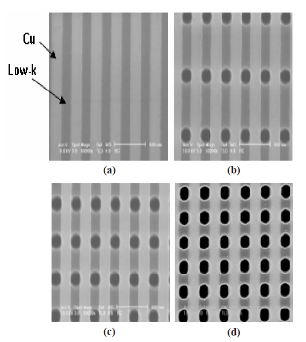
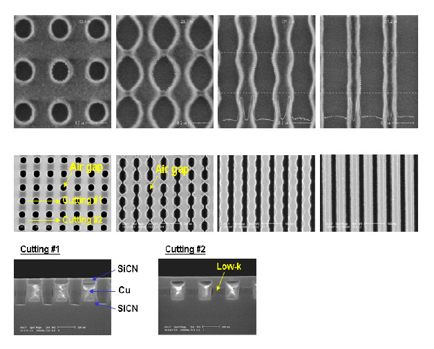
This study proposes the via-typed air-gap to overcome the problems of the trench-typed air-gap. Figure 1(a) depicts the repetitive hole patterns on the ILD area between metals. The k-value can be easily adjusted by the porosity with the ratio between hole size and space length, because the dielectric constant of air is k = 1, as shown in Fig. 1(b). Figure 2 shows the experimental results of the depiction in Fig. 1, which arranges the SEM images
after performing photolithography and etching processes. Various shapes of air-gap could be formed by changing the hole size and space distance. The trench-typed air-gap could be fabricated when the space shortens. The dark area in the SEM images of the etching specimens is the air-gap. When the air-gap formation area (cutting #1) and the low-k remaining area (cutting #2) were observed using the X-SEM, the experimental results matched the expectation in Fig. 1.
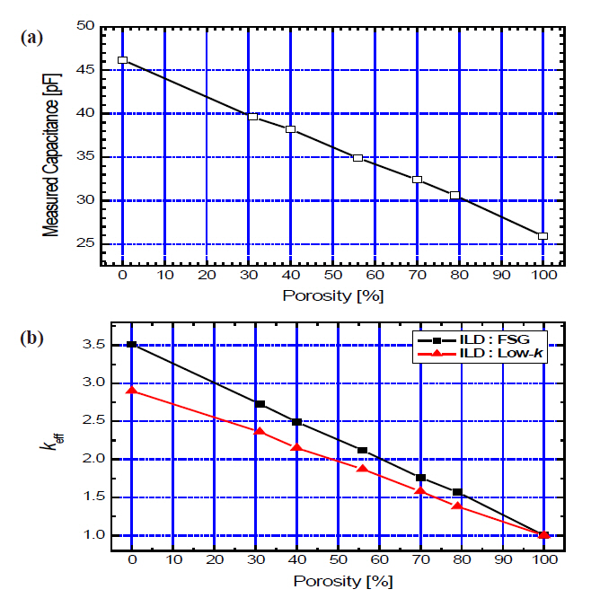
Various ULK were fabricated with a change of space-distance. Figure 3(a) shows the completed metal interconnects before forming the air-gap. The via-typed air-gaps of 132 nm-diameter were formed by the hole etching process with each spacedistance of 367, 190 and 97 nm, respectively; the holes between metal interconnects were formed and well arranged, as shown in Figs. 3(b-d). The parasitic capacitance of the fabricated viatyped air-gaps was measured in the comb pattern, while the low-k as an ILD was used with the dielectric constant of k = 2.9.This can be estimated as k = 1, because all of ILD between metals were removed, having etched for the trench-typed air-gap. The measured capacitance is expressed as a function of porosity in Fig. 4(a). The measured capacitance could be converted into the effective k value from the relational expression of C = k·0 A / d,as shown in Fig. 4(b), where k is the dielectric constant, 0 is the permittivity of free space, A is the plate area and d is the plate separation. This denotes ULK can be fabricated and controlled easily by the via-typed air-gap. The trench-typed air-gap could be also easily implemented using the hole patterning. The ILD deposited via-typed air-gap to form the upper interconnects showed superior performance to the trench-typed air-gap. The ideal formation of the air-gap is maintained as the air-gap only in the area with the much parasitic capacitance due to the short space distance. However, usually the air-gap approaches the upper layer in the case of the non-conformal dielectric. The defect can be caught in the lower air-gap layer, if upper air-gap cleaning is not sufficiently good. Therefore, the yield can be drastically reduced.This may penetrate the air-gap in the lower layer. Therefore,the yield is drastically reduced. Recently, the vertical design
rule, as well as the horizontal design rule, is strongly required to be scaled-down but it is very difficult to develop the technology,since the vertical design rule cannot be reduced if the air-gap is near the upper interconnects.
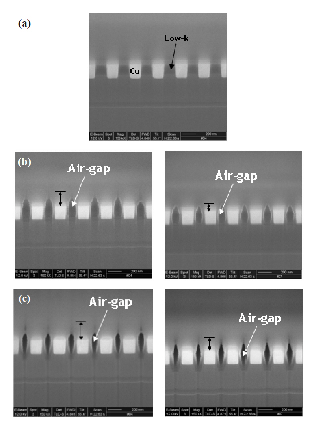
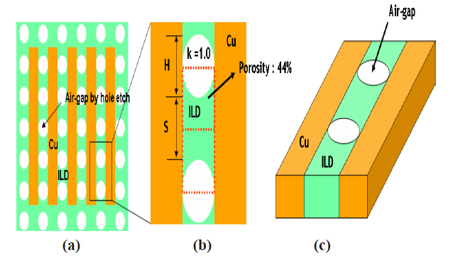
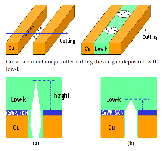
The via-typed air-gap can be a powerful solution for the problem mentioned previously, by comparing the trench-typed airgap analyzed with a focused ion beam, as shown in Fig. 5. Figure 5(a) shows the Cu/low-k interconnects without the air-gap, while Figs. 5(b) and (c) show the interconnects with the air-gap. The air-gap heights were compared to each other in the two cases.The height of the air-gap was defined as the height when the airgap disappeared from the top of the Cu metal in the lower layer.The difference in the height of the air-gap was examined, which occurs having deposited only the low-k as an upper ILD upon after the hole patterning and having deposited SiCN as a barrier dielectric material before deposition of low-k. The height of the via-typed air-gap was reduced by 50% compared to that of the trench-typed air-gap, as shown in the lower part of Fig. 5(b). Figure 6 briefly explains the principle of this phenomenon. It is considered that the height when the air-gap disappeared was high in the formation of the trench-typed air-gap, because the deposited material grows in two directions, while the height in the formation of the via-typed air-gap was low, because the deposited material grows in four directions. That is, this denotes the via-typed air-gap can be applied to devices with low height of via in the upper layer. The trench-typed air-gap generally shows an insufficient level of misaligned margin in the area with the dense and narrow lines of the line-width due to the air-gap near the upper part. Therefore, it is very difficult to design the devices, because the bridge may be generated by contacting the air-gap when the via is opened. However, the critical problem in device design will be solved with the via-typed air-gap due to no limited location of via-typed air-gaps onto the low-k without air-gap in the lower layer, since the via-typed air-gap can be arranged through crossing the air-gaps of the N+1th metal line over the air-gaps of the Nth metal line.
The controllable ULK was easily fabricated through the viatyped air-gap. The trench-typed air-gap could be also formed by adjusting the hole density. The via-typed air-gap overcame the problem of uncontrollable k-value in the trench-typed airgap.The air-gap height approaching the upper layer could be reduced by about 50% for the vertical design rule using the viatyped air-gap. The highly-integrated design of devices might be easily applied to the area with dense and narrow lines by the viapatterning,because the via-typed air-gap could be formed by crossing each layer.