The successful application of optical transmission technology to long-distance and short-distance communication systems has enabled today’s ultrahigh speed mass communication. In recent years, the optical printed circuit board (O-PCB), a new concept wherein optical signal transmission technology is applied to a printed circuit board (PCB), has been proposed and developed [1-4], and is expected to be commercialized in the near future.
In general, O-PCBs are classified into rigid and flexible types, and the flexible type is often referred to as a flexible optical circuit board (FOCB). In a FOCB, an embedded flexible optical waveguide is the most important constituent, determining the transmission efficiency and the transmission distance of the FOCB. For commercialization of O-PCBs, it is important to evaluate the quality of the optical waveguide including inspection of its internal structure. While many methods are available to inspect the surface profile or the internal structure of an optical waveguide [5, 6], most of them are destructive or contact methods. However, a confocal microscope [7, 8] can provide high lateral and longitudinal resolutions by using a point source and a point detector. Furthermore, it has a special optical sectioning property that enables internal inspection of three dimensional structures[9-11]. Accordingly, the confocal microscope is believed to be a useful tool for O-PCB evaluation, since its characteristics enable noncontact and nondestructive inspection of an optical waveguide.
In a confocal microscope, the 3-dimensional information of a transparent sample is measured by detecting the light reflected from either defects or material interfaces within the sample and gathering the signal over the sample. For the case of measuring a transparent optical waveguide, however, the light reflected from the internal material interface is very weak due to the very small refractive index difference. Therefore, it would be difficult to measure the internal structure of an optical waveguide with a conventional confocal microscope.
In order to resolve this difficulty, we propose a new method for enhancing the light reflection from material interfaces:using an oil-immersion lens and a theta microscopy scheme[12-17]. In section II, the structure and properties of the flexible optical waveguide used in this study are explained,and the internal structure measured with a conventional confocal microscope is shown. In sections III~IV, the proposed method is introduced and its operational principle is explained, and finally experimental results and their implications are discussed.
II. AN OPTICAL WAVEGUIDE MEASURED WITH A CONVENTIONAL CONFOCAL MICROSCOPE
2.1. An Optical Waveguide Embedded in a FOCB
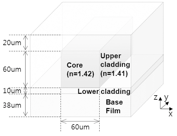
The structure of an optical waveguide embedded in a FOCB is depicted schematically in Fig. 1. The waveguide is composed of an upper cladding layer, a lower cladding layer, a square-shaped core (about 60×60 ㎛2) surrounded by the two cladding layers, and a transparent base film supporting the waveguide structure. All layers are made of ductile synthetic resins and their dimensions are specified in Fig. 1 in detail. The refractive indices of the core and cladding materials are 1.42 and 1.41, respectively, giving an index difference of 0.01. In Fig. 1, the waveguide axis and the direction normal to its constituent layers are denoted as the y and z axes, respectively. The FOCB to be measured was mass-produced by a roll-to-roll process, where the formation of a lower cladding layer on a base film, the formation of a core structure by hot embossing, and the formation of an upper cladding layer by curing were accomplished sequentially.
2.2. Measurement of the Optical Waveguide with a Conventional Confocal Microscope
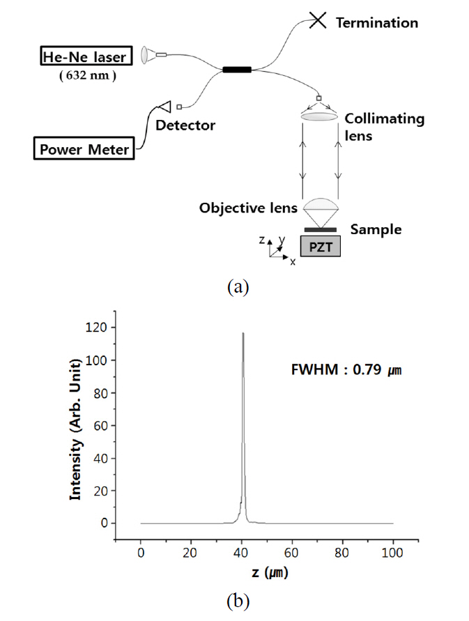
As shown in Fig. 2(a), a conventional confocal microscope was constructed for investigating whether the internal structure of the optical waveguide could be observed. Since the scheme of a fiber optical confocal scanning microscope(FOCSM) is employed [18, 19], the light beam emitted from a light source is coupled into one input port of a 3-dB fiber-optic coupler and is split into two beams toward two output ports. The light emanating from one output port of the coupler is focused to a sample via a collimating lens and a microscope objective lens. The light beam reflected from the corresponding focusing spot is coupled back to the cross-section of the same output port, and finally is measured by a detector. Because the fiber-optic coupler substitutes for both the beam splitter and the pin hole of a conventional confocal microscope, the FOCSM can be simply constructed and easily aligned. However, use of the coupler results in unwanted light reflection, mainly caused from its coupling region and/or its fiber end face, and thus tends to worsen the signal-to-noise ratio (SNR) and the signal contrast of the system. In particular, when a coherent light is used as a source, the signal fluctuation may be caused by mutual interference of unwanted light with the signal light.
As shown in Fig. 2(a), a He-Ne laser (wavelength 632.8 nm) and a Si detector were used as a light source and a detector, respectively. A microscope objective lens (Nikon,CF Plan EPI 81804) with a NA of 0.95 and magnification of 100 was used. All fiber ends of the fiber-optic coupler were index-matched to minimize light reflection from their end faces. A PZT stage system for scanning a sample 3-dimensionally has identical moving ranges of 100 ㎛ and identical moving step sizes of 10 nm for all axes. The microscope system was controlled by a computer via a general purpose interface board (GPIB). In order to investigate the performance of the constructed system, the axial response curve was measured by using a mirror plate instead of a sample. From the response curve shown in Fig. 2(b), the full width at half maximum, representing the vertical resolution of the constructed FOCSM, was measured to be approximately 0.79 ㎛.
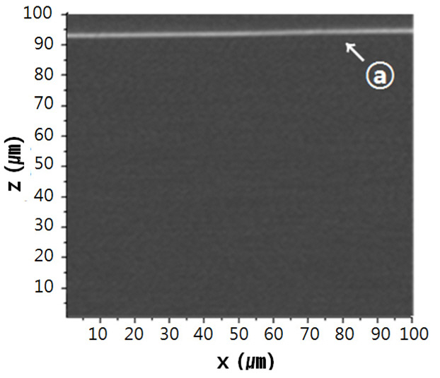
Next, the FOCB was mounted on the sample stage in order to observe the internal cross-section of one optical waveguide, and its waveguide axis was aligned to be parallel to the y axis of the stage. Although all sectional images were obtained by scanning the FOCB 3-dimensionally, no other internal interfaces except for the air-upper cladding interface were observed. As an example, the xz-sectional image normal to the waveguide axis is shown in Fig. 3, where the air-upper cladding interface is indicated by the symbol ⓐ.
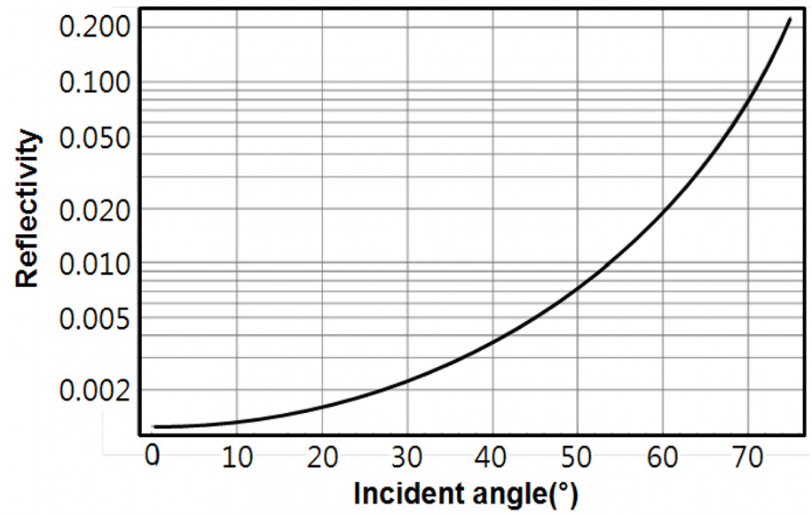
The failure to observe any internal material interfaces is thought to be attributable to the low SNR of the FOCSM, which in turn stems from the very small index difference between the constituent materials. Considering the NA of the objective lens used and the incidence of the probe beam from air, the light reflected from the material interfaces would be very weak, and consequently it could not be distinguished from the light reflected from internal defects, including index inhomogeneity or any other noisy lights. In order to clearly elucidate the weakness of the light signal, the reflectivity of the core-cladding interface in accordance with the incident angle was calculated and the result is shown in Fig 4. Since the incident angle of the probe beam focused by the objective lens ranges roughly from 0° to 42°, even the most inclined probe beam has a very low reflectivity of around 0.0045% and the overall reflectivity of the probe beam becomes less and less. Accordingly, a method for enhancing the light reflection from the internal interfaces is required in order to observe the internal cross-sections and interfaces of a transparent optical waveguide.
III. A METHOD PROPOSED FOR ENHANCING THE SIGNAL CONTRAST
In this paper, a method is proposed to enhance the reflectivity of the probe beam at material interfaces within the optical waveguide, and thus to observe the internal crosssection of a transparent optical waveguide embedded in a FOCB. The main ideas of the proposed method are to widen the incident angle range of the probe beam by using a microscope objective lens with a higher NA and to increase the average incident angle of the probe beam by inclining the probe beam with a theta microscope scheme.
An oil-immersion objective lens has often been used for enhancing the resolution of a confocal microscope, and it can also widen the incident angle range of the probe beam due to its high NA. Accordingly, the objective lens used in the setup shown in Fig. 2(a) was replaced with an oil-immersion lens (Nikon, Plan Apo VC MRD01901) whose NA and magnification were 1.40 and 100, respectively. By using this lens with a higher NA, the incident angle range of the probe beam was widened further, and consequently the reflectivity of the core-cladding interface could be increased to 0.2% at most, as estimated from Fig. 4. Therefore, the intensity of the light reflected from the material interfaces would be increased further compared to that obtained using the previous lens.
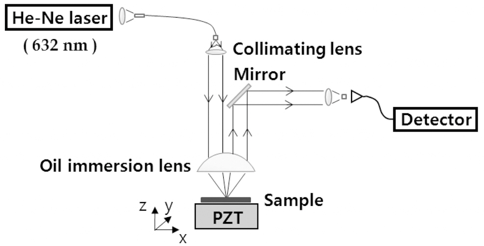
In order to increase the average incident angle of the probe beam, a theta microscope type-confocal microscope was established, as illustrated in Fig. 5. In this configuration, the probe beam is incident on the edge of the microscope objective lens, and the reflected beam will be detected after coming out through the opposite edge of the lens. Because the light paths of the incident probe beam and the reflected beam are different from each other, the fiber-optic coupler cannot be used any more. By constructing the confocal microscope based on a theta microscope type, the probe beam is obliquely incident to internal material interfaces, and thus the reflected light intensity can be increased due to this oblique incidence. Additionally, there is an advantage of enhancing SNR, because there is no need for the fiber-optic coupler, which generates unwanted reflected light.
IV. MEASUREMENT OF AN OPTICAL WAVEGUIDE WITH THE PROPOSED METHOD
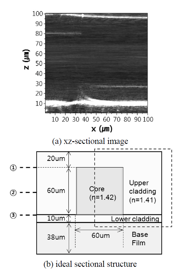
First, the internal structure of an optical waveguide was measured with the confocal microscope using an oil-immersion lens only. With a scanning FOCB mounted on the sample stage, the intensities of the reflected light were detected over the whole scanning region and sectional images were reconstructed from the 3-dimensional intensity distribution. The xz sectional image of the optical waveguide is shown in Fig. 6(a), and the xz cross-section of the initially designed waveguide is schematically shown in Fig. 6(b) for comparison. The sectional image corresponds to the dotted box drawn in Fig. 6(b), and has a size of 100 ㎛ × 100 ㎛ and a pixel resolution of 200 × 200, with scanning steps along the x and z axes of 500 nm. In Fig. 6(a), the top white line and the short white line below it represent the shapes of the air-upper cladding and the upper claddingcore interfaces, respectively. The bottom thick white line and the short white line just above the thick line represent the existence of the lower cladding-base film and the upperlower cladding interfaces, respectively. Since the FOCB was mass-produced by a roll-to-roll process, as already mentioned, and the final upper cladding layer was formed by coating a liquid cladding material over the core structure, the air-upper cladding interface inevitably takes a curved shape. The lower cladding layer is thought to be thicker than the designed waveguide due to the inaccurate fabrication process. Even though the details of the measured waveguide are different from those of the ideal waveguide, all interfaces except for the core-lower cladding interface can be clearly measured with a confocal microscope using an oil-immersion lens.
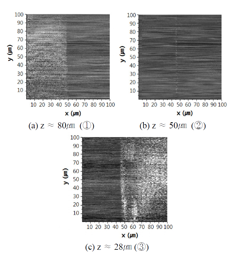
In order to check whether the sidewall boundary of the core could be observed, three xy sectional images were reconstructed from the same intensity distribution. The first xy sectional image shown in Fig. 7(a) represents the intensity distribution at the height denoted as ① in Fig.6(b) (z=80 um), where the upper cladding-core interface is located. The left and the right sides of Fig. 7(a) correspond to the upper cladding-core interface and the interior of upper cladding layer, respectively. Since the intensity of the light reflected from the upper cladding-core interface is stronger than that of the light that is returned from the interior, the left side is seen to be brighter than the right side. The vertical line observed in the middle of Fig. 7(a) reveals the existence of the sidewall between the core and the upper cladding layer.
The second xy sectional image shown in Fig. 7(b) represents the intensity distribution at the height denoted as ② in Fig. 6(b) (z=50 ㎛), which corresponds to the middle height of the sidewall. Since no interfaces are located on the plane, a relatively bright region is not observed in the figure, but the central line representing the sidewall boundary is seen.
The last xy sectional image shown in Fig. 7(c) represents the intensity distribution at the height denoted as ③ in Fig. 6(b) (z=28 ㎛). The left and the right sides of this plane correspond to the core-lower cladding interface and the upper-lower cladding interface, respectively. If the FOCB has been fabricated correctly, the index difference of the core-lower cladding interface will be larger than that of the upper-lower cladding interface, and accordingly the left side of Fig 7(c) is expected to be brighter than the right side. However, the sectional image reveals the opposite result, contrary to expectations. This means that the refractive indices of the two cladding layers may not be identical or the index difference of the core-cladding interface may be smaller than expected. Considering that the cladding layer has been formed by thermal or UV curing, this result is believed to stem from the index difference of the two cladding layers.
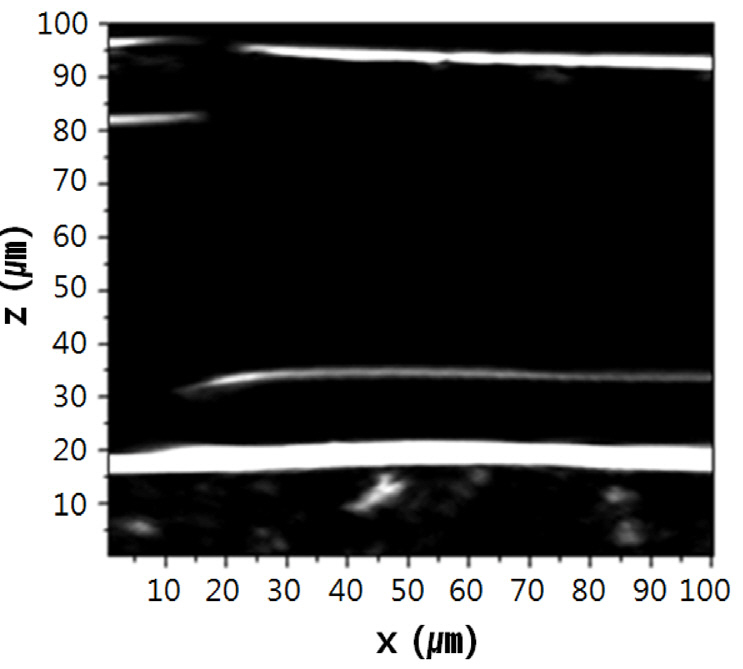
Finally, the proposed method, illustrated in Fig. 5, was applied to measure the internal structure of the optical waveguide more clearly, and the measured xz sectional image is shown in Fig. 8. The measuring conditions were the same as with the previous measurement except for incorporation of the theta microscope scheme. Since a fiber-optic coupler was not used with the theta microscope scheme, unwanted light reflection from the coupling region and fiber end face of the coupler does not occur. Accordingly, the sectional image reveals the shapes and the positions of all material interfaces within the optical waveguide with high signal contrast.
The internal structure of a transparent optical waveguide made of constituent materials with very small index differences was successfully observed with the confocal microscope with enhanced signal contrast. The signal contrast of a confocal microscope was enhanced by using an oil-immersion microscope objective lens with an ultrahigh NA and combining a theta microscope scheme into a conventional confocal microscope. The proposed method provided a higher signal contrast than that obtained using an oil-immersion objective lens only.
By measuring the shapes and the dimensions of internal material interfaces such as the core-cladding interface and the sidewall of the core, the optical waveguide embedded in a FOCB could be inspected. Since the method based on a confocal microscope is nondestructive and noncontact, it will be useful tools for evaluating FOCBs and controlling the fabrication process.