Plasmonic waveguides have attracted great attention for deep subwavelength confinement beyond the diffraction limit compared to conventional dielectric-based ones [1, 2]. The rising interest in such waveguides lies in the fact that their propagation modes have decay lengths that are perpendicular to the propagation direction and are much smaller than the excitation wavelength. They are considered as alternatives applicable to highly integrated photonic circuits such as filters[3], modulators [4], sensors [5, 6], optical attenuators [7] and switches [8]. However, highly confined modes involve enhanced propagation losses that are typically due to Ohmic loss in the metal and therefore there is a fundamental trade-off between light confinement and propagation loss.
In recent years, surface plasmon polaritons (SPPs) in the metal slot have been thoroughly investigated and reported to feature a well-balanced tradeoff between localization and propagation loss [9-16].
In this paper, we investigate the fundamental waveguide parameters of slot waveguides at the telecom wavelength(1550 nm) such as an effective refractive index, propagation length and figure of merit (FOM) including both the confinement and loss effects previously reported [15]. First, we investigate the effects of variation in slot thickness and width on mode confinement and propagation length. Furthermore, an efficient design approach is provided to obtain a slot waveguide with optimal performance parameters. We will optimize the waveguide geometry by using the genetic algorithm(GA). Through the analysis and design procedure, we identify the intrinsic tradeoffs and suggest an optimal geometry of a plasmonic waveguide with considerable propagation length and deep-subwavelength localization with strong field enhancement.The field analysis will be carried out through the finite element method (FEM).
II. ANALYSIS OF PLASMONIC SLOT WAVEGUIDES
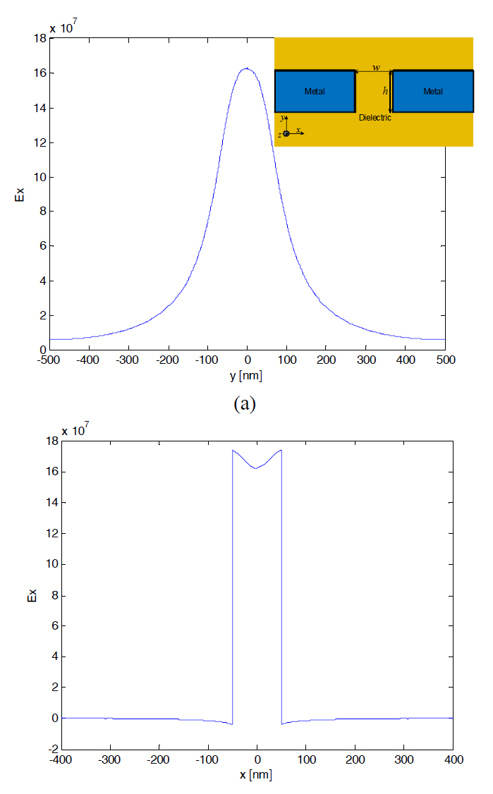
The geometry of a plasmonic slot waveguide is shown in the inset of Fig. 1 (a). It consists of a slot in a thin metallic film with width
Fig. 1(a) shows the vertical field distribution of the dominant electric-field component along the center of the slot with
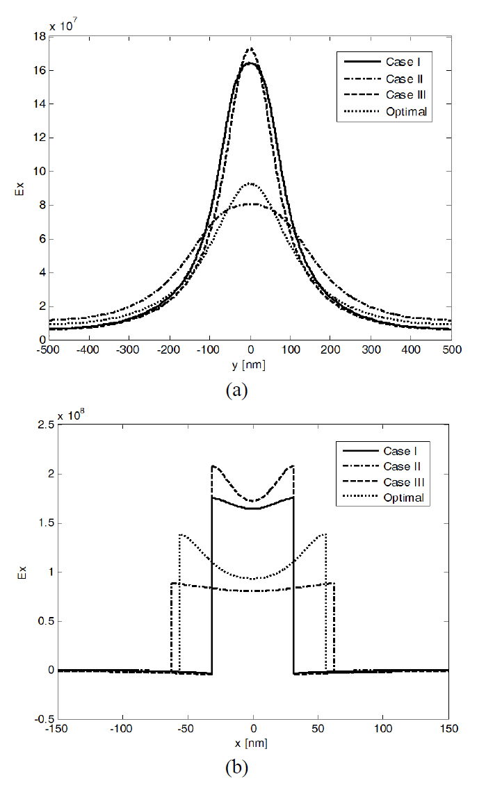
In Fig. 1(b), we show the lateral distribution of the dominant electric-field component along the center of the slot with
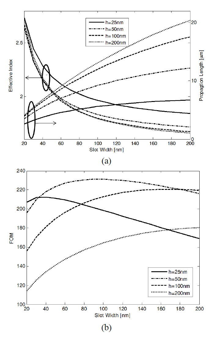
We first investigate the effect of the slot dimension on the propagation characteristics. In Fig. 2 (a) we show the effective index
, which is similar to the proposal in [15]where
In Fig. 2 (b) we show the FOM of the propagation mode
of the slot plasmonic waveguide as a function of the slot width w for different slot thicknesses. Unlike
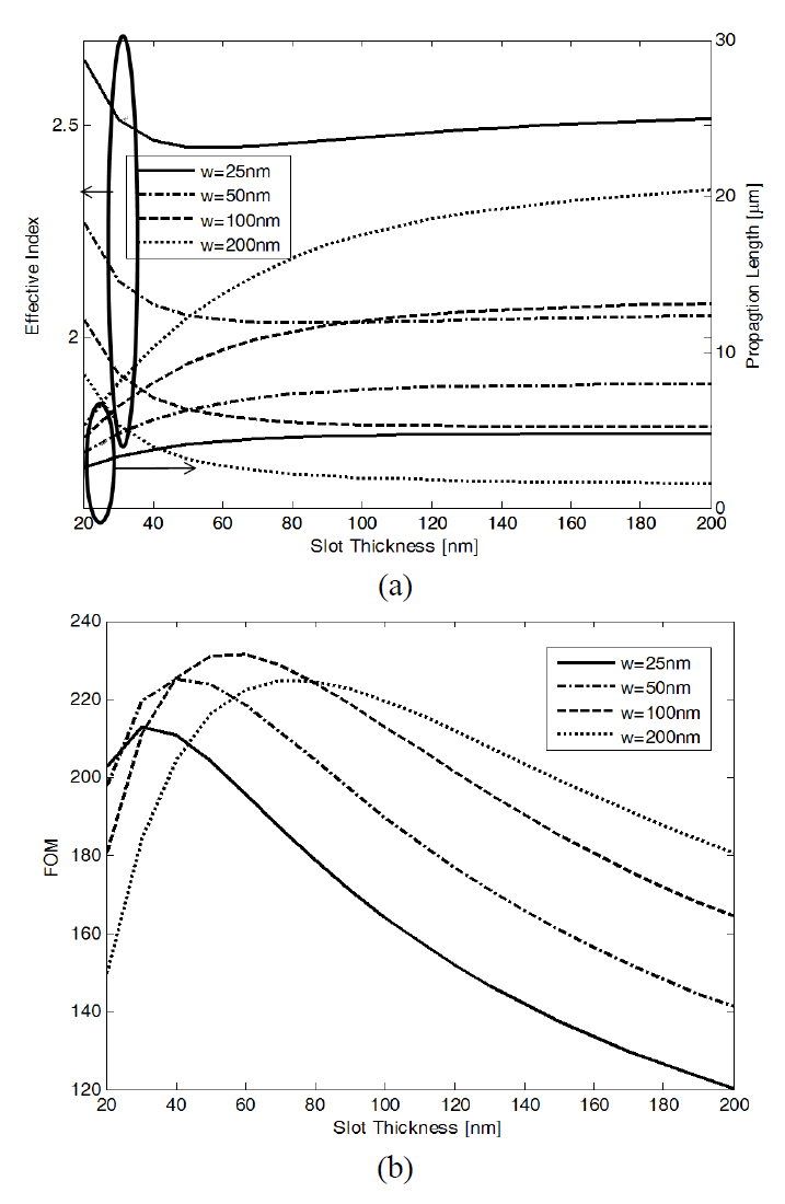
In Fig. 3 (a) we show
In Fig. 3 (b) we show the FOM of the fundamental mode of the slot waveguide as a function of slot thickness according to slot width. It is clear that the FOMs are not monotonic,but reach a maximum around 30-100 nm, and this is therefore a local maximum. In these cases, an optimization approach based on gradient, e.g. sequential quadratic programming(SQP), would be more likely to obtain a local maximum and depend on its initial value.
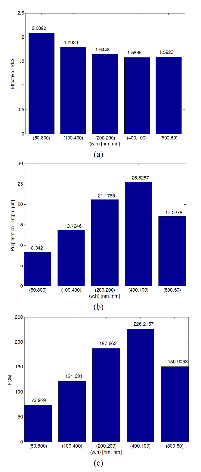
In Fig. 4 (a), (b), and (c) we show
III. OPTIMAL DESIGN USING GENETIC ALGORITHM
The GA approach is applied to the optimization of the plasmonic slot waveguide in order to design waveguide parameters. The GA is a powerful and efficient method for optimization problems of a given function with many design parameters. It is based on a stochastic technique, and a population of individuals is randomly created at each generation.In our computations, the objective function is FOM, as previously defined, and the design parameters are the width
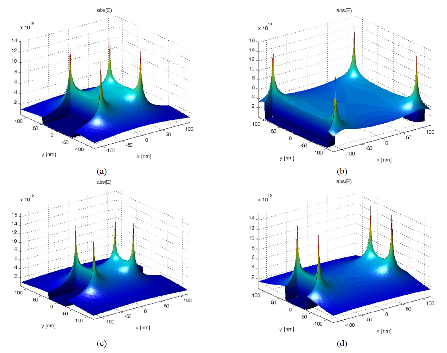
Fig. 5 shows the electric field distribution of the plasmonic slot waveguides for the different cases in Table 1. The numerical results show that the mode profile is confined around the corners of the slot. Their field distributions remain fundamentally unchanged with the exception of a slight change in mode confinement and corresponding propagation length,whereas there are considerable changes in FOM values.
In Fig. 6 (a) and (b), we show the vertical and lateral distribution of the dominant electric-field component along the center of the slot for the different cases in Table 1,respectively. Comparing the optimal case with cases I-III,it is clear that in the optimal case, the mode confinement is higher than for case III, but its FOM is the maximum,because in case III, the propagation length is much shorter.
[TABLE 1.] Optimum parameters of the GA
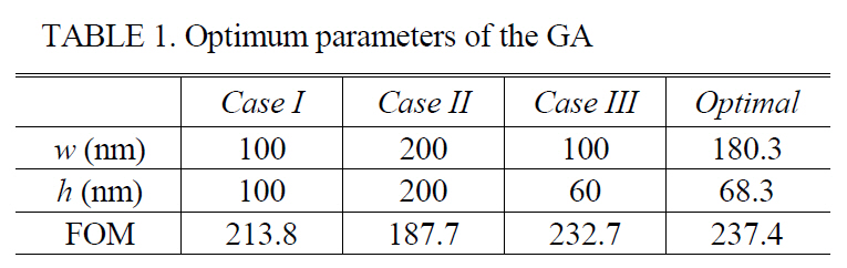
Optimum parameters of the GA
A numerical study of propagation characteristics of the plasmonic slot waveguide has been performed. We used the FEM and investigated the effect of the slot dimension on propagation characteristics such as the effective refractive index, propagation length and FOM including both confinement and loss effect. The field distributions of the propagation mode for the slot waveguide were investigated numerically in detail. Furthermore, using GA, we presented an efficient and powerful approach to the optimization of the plasmonic slot waveguide for high mode confinement and long propagation length, between which there is an intrinsic tradeoff.The approach proposed here has important implications for designing optimal plasmonic waveguides applicable to highly integrated nanometric optical circuits.