검색 전체 메뉴
PDF
맨 위로
OA 학술지
Duality of Photonic Crystal Radiative Structures and Antenna Arrays
  • 비영리 CC BY-NC
  • 비영리 CC BY-NC
ABSTRACT
Duality of Photonic Crystal Radiative Structures and Antenna Arrays
KEYWORD
Photonic crystal waveguide , CROW , FDTD , Resonator , Antenna arrays , (230.0230) Optical devices , (130.3120) Integrated optics devices , (230.1360) Beam splitters , (140.4780) Optical resonators
  • I. INTRODUCTION

    The beam shaping mechanisms of optical fields have attracted many researchers from the beginning of the study of electromagnetic fields [1-17]. Recently, it has been shown that beam shaping could be achieved by different kinds of photonic crystal structures due to their photonic band-gap properties [1-13]. One of the methods of beam shaping is engineering the surface modes via corrugations of the surface layer of the photonic crystal waveguide and appropriate termination of the waveguides [11, 18-21]. The defect placement, either point or line defects, at the termination side of the waveguide, modifies the pattern of the radiative beam [22-25]. For these kinds of photonic crystal structures, the mechanism of beam shaping is that the resulting optical field distribution at the photonic crystal exit resembles a multiple point source. The defect types and the arrangement of them, as point sources, cause a particular shape of light emission. The main aim of these studies is designing a particular radiative beam shape at the output of the photonic crystal structures, for example eliminating the side lobes and reducing the divergence angle of the main lobe to increase the directivity for better matching, or splitting the emitted beam for dividing the output light of the photonic crystal device to the next photonic crystal or conventional device in photonic integrated circuits (PICs) [8].

    Photonic crystal resonators are special optical components for photonic integrated circuits (PICs). Coupled resonator optical waveguides (CROWs) are constructed with a chain of strongly confined ring resonators [26-29]. The pattern of emitted beam from a CROW surface of a photonic crystal waveguide shows the focusing effect [8].

    These remind us of the behavior of the antenna arrays which makes it possible to derive more directional characteristics.The total field of the array is determined by the vector addition of the fields radiated by the individual elements.To provide very directional patterns, it is necessary that the fields from the elements of the array interfere constructively in the desired direction and interfere destructively in the remaining space [30-33].

    In this paper, we have used the two dimensional finite difference time domain (FDTD) method to derive the pattern of the photonic crystal radiative defect arrays, and we compare the behavior with that of the antenna arrays.

    II. DETAILS OF STRUCTURES AND SIMULATION SPACE

    We have considered a photonic crystal structure with a square lattice of dielectric rods in air. The relative dielectric constant of the rods is 11.56, corresponding to the relative dielectric constant of InGaAsP-InP semiconductor at 1.55㎛ wavelength [8], and the cross-sectional radius is chosen to be 0.18a, where a is the PC lattice constant. For TM polarization with the electric field parallel to the rod axis, the photonic band-gap of the photonic crystal structure is in the normalized frequency (ωa/2πc) range of 0.306-0.439,as can be derived by either of the two methods of broadband Gaussian pulse excitation and plane wave expansion(PWE), where ω is the angular frequency, and c is the velocity of light in free space. All results are presented for TM polarization and have been obtained by the 2D-FDTD method with perfectly matched layer boundary conditions.We have considered Δx = 2r/10 as the spatial step in the FDTD method, where r is the cross-sectional radius of the rods. We have chosen radiative defects, by removing some rods at regular intervals at the photonic crystal termination. In this structure each resonator can radiate to free space.The total field of the array is determined by the vector addition of the radiated fields of the individual resonators,the result of which is the radiation pattern of the structure.

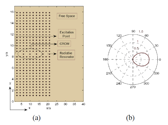
    In this paper, we have demonstrated the duality of the two structures of radiative photonic crystals, and antenna arrays. But there are some differences. First, the radiative field of a resonator is not analytically known. So, we cannot derive a formula, as in antenna arrays, for total radiative fields of the structure. Second, due to some mutual coupling of the resonators, despite the antenna array, the amplitude relation and the phase differences between the resonators are somehow out of our control. To overcome these two effects, we have used the FDTD method in a large space to calculate the far field, and for the latter we have chosen the distance between the resonators as large as to prevent the mutual coupling. Each resonator is excited by a separate source at the entrance of the waveguide linked to the resonator.Because of the similarity of each resonator excitation, the phase difference can be supposed to be zero. As an example FIG. 1 (a) shows the excitation point, CROW, and the radiative resonator for a single element radiative array, and FIG. 1 (b) shows its pattern, as the unit pattern in an antenna array that is mentioned in Appendix A.

    The source is a modulated Gaussian:

    image

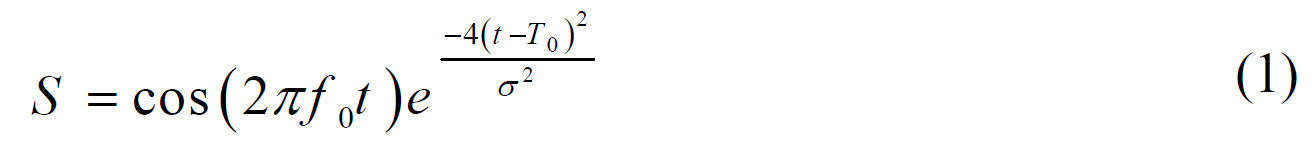
    where f0 is the resonant frequency of the resonator, t is time, T0 is the time of the peak and σ is the width controller of the Gaussian pulse.

    The normalized resonant frequency of the resonator (ωa/2πc) is 0.396, derived by launching an impulse source (very narrow Gaussian source that its frequency spectrum contains the total band-gap of the photonic crystal) to a photonic crystal waveguide without and with a resonator near it. The resonant frequencies are coupled to the resonator. Thus,the Discrete Fourier Transform (DFT) of the waveguide output at resonant frequency is decreased. So, we can get the resonant frequencies, as shown in FIG. 2.

    In order to restrict the interference of the non-resonant frequencies in free space, we choose σ for a narrow spectrum bandwidth, to approach the monochromatic lightwave signal.Moreover, to achieve the more pure resonant frequency in the radiative resonator, we use CROW to link the excited points to the radiative resonator, due to the filtering behavior of CROW.

    In this paper, the FDTD software was prepared in C++ and MATLAB and was carried on a Pentium 4 computer with processing capacity of 2.84 GHz and 3.25 GB of RAM.

    III. THE COMPARISON BETWEEN PHOTONIC CRYSTAL RADIATIVE STRUCTURES AND ANTENNA ARRAYS

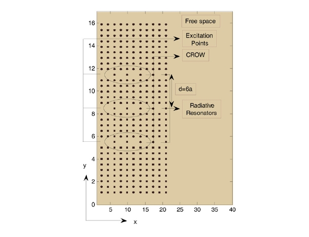
    We have considered several photonic crystal radiative arrays by repeating FIG. 1 (a) structure in regular intervals of various multiples of a as arrays element spacing, and arbitrary numbers of array elements. The element distance was chosen such that the coupling between the radiative elements was negligible. As an example, FIG. 3 depicts an array with radiative elements number of N = 3, and elements distance of d = 6a. Then, we excited each of the resonators of the arrays with two types of uniform and binomial excitations. As explained in Appendix A, in the uniform excitation, the incident signals of all CROWs launched to the resonators are the same as Eq. (1), but in the binomial excitation the amplitude of each signal is a multiple of Eq.(1), the multiplication factor of which is chosen from FIG.A. 1. For example in FIG. 3, the excitation of middle CROW is two times greater than that of the bottom and top CROWs. So, as the excitation of each resonator is similar, the phase differences between the elements are supposed to be zero

    We have placed some detection points in free space at distances further than 10λ say D=30a from the center of

    the array. The detection points are assumed to be at the angle of -90° to 90° with an angle interval of 3°. The amplitude of the electric fields of the detection points gives the total pattern of the arrays.

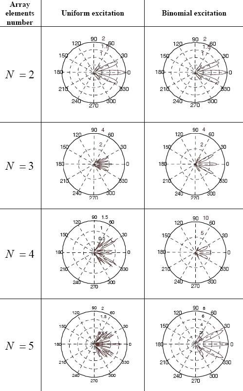
       3.1. Effects of Variations of The Number of Radiative Elements

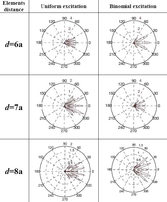
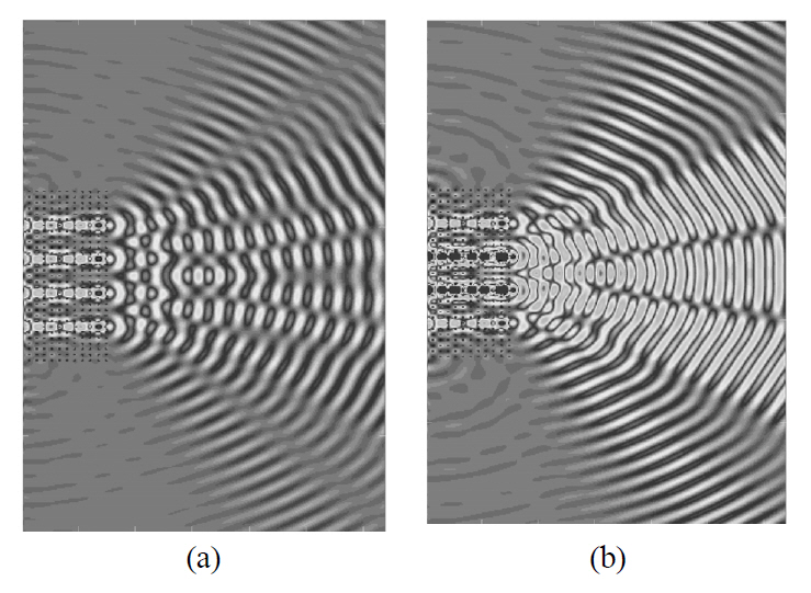
    TABLE 1 shows the total pattern for an N-element array for various numbers of N and specified element distance d, for uniform and binomial excitation. The field pattern formula is the product of the array factor and the unit factor shown in FIG. 1. (b), as those of antenna array given in Appendix A. The same as for antenna arrays in uniform excitation, for a certain d, as the array element number (N) is increased, the main lobe direction is constant,but its width becomes narrower, and the number of secondary or minor lobes is increased. These results are in good agreement with the similar case in antenna arrays,given in Appendix A. But there is some exception in these

    figures such as N=4. This is because of the effect of partial coupling between the radiative resonators, variation of the resonant frequency of single resonator and CROW that cause undesirable radiation by non-resonant frequency in free space, and the possibility of changing the phase of each radiative element in CROW path.

    In the binomial excitation, as shown in TABLE 1, the same as antenna arrays, given in Appendix A, the minor lobes are eliminated. By increasing N, for a certain d, in contrast to the uniform case, the number and direction of lobes, do not change, their intensities are increased and hence the directivity is enhanced. But, for the same number of photonic crystal radiative structures, the lobe-widths are more than those of the uniform one. These are again the same as the results for antenna arrays, given in Appendix A. The optical field distributions of a 4-element array with element distance of d=6a for both excitations of uniform and binomial, are demonstrated in FIG. 4.

       3.2. Effects of Variations of The Elements Distance

    TABLE 2 depicts the patterns of a 3-element array for different distances for uniform and binomial excitations. In uniform excitation, for a given N, if the elements distance is increased, the direction of the main lobe is changed, the main lobe becomes narrower, and the number of secondary or minor lobes is increased.

    In the binomial excitation, as shown in TABLE 2, for a given N, by increasing d, the number of lobes is increased,the directions are changed, and the lobe-widths are decreased.

    All the results follow the same variations as those of antenna arrays, described in Appendix A. The reasons for some minor exceptions are the mutual coupling between the photonic crystal CROWs, variation of the resonant frequency of single resonator and CROW that cause undesirable radiation by non-resonant frequency in free space,and the possibility of changing the phase of each radiative element in CROW path.

    We have analyzed more cases of photonic crystal radiative arrays with various N and d for uniform and binomial excitation and found a considerable duality with antenna arrays. So this duality can be generalized to the other types of excitation such as Dolph-Tshebyscheff arrays, and to the other arrangement of radiative resonators such as any linear, planar and circular arrays of 3D photonic crystal termination resonators.[33] We expect that these structures behave like their equivalent antenna arrays.Therefore, all the experiences in antenna array designs can be employed for manufacturing the photonic crystal beam shaping devices. These devices are very significant in photonic integrated circuits (PICs), due to their capability for enhancing the directivity or splitting the output beams of the photonic crystal devices to be matched to the following devices with single or multiple input ports,respectively, to reduce the connection loss.

    IV. CONCLUSION

    In this paper, we have compared the behavior of photonic crystal radiative structures and antenna arrays for two types of uniform and binomial excitations. We found that there is a considerable duality between them. We can generalize the results to the other types of excitations such as Dolph-Tshebyscheff arrays, and to the other arrangement of radiative resonators such as any linear, planar and circular arrays of 3D photonic crystal termination resonators.Therefore, all the experiences in antenna arrays can be employed in manufacturing the photonic crystal beam shaping devices, in order to reduce the divergence of main lobe to enhance the directivity for better coupling, or splitting the emitted beam in order to divide the output beam to the next devices in photonic integrated circuits (PICs).

    APPENDIX A. AN OVERVIEW OF BEAM SHAPING IN ANTENNA ARRAYS

    There are at least five parameters and characteristics for shaping the overall pattern of the antenna arrays. These are the geometrical configuration of the overall array (linear,circular, rectangular, etc.), the relative distances of the elements, the excitation amplitude and phase of the individual elements, and the relative pattern of the individual elements.

    The simplest and one of the most practical arrays are formed by placing N antenna elements along a line. For a uniform amplitude and spacing, the total field can be determined by multiplying the array factor (AF) of the isotropic sources by the pattern of the single element,called unit factor (UF). Array factor can be expressed in an alternate, compact and closed form [33]:
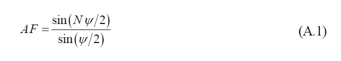
    image

    where ψ =α +βd cosθ, where α is the phase difference between the elements, β is the propagation constant, d is the elements separation, θ is the angle of view and N is the number of array elements. Thus the array factor is a function of the number of elements, their geometrical arrangement, their relative phase, and their distance. By varying the number of elements N, distance d and/or the relative phase α between the elements the characteristics of the array factor and the total field of the array can be controlled.

    For ψ = 2/N , k = 1, 2, 3,… the array factor has nulls,and for ψ = 2kπ , k = 0, 1, 2, 3,… . Eq. (A.1) attains its maximum values. Thus the number of nulls that can exist will be a function of the number of elements N, element distance d and the phase excitation difference α. Here, we suppose α to be zero and consider the effects of the variations of the other parameters. Thus, for uniform excitation,for a certain d, as the number of array elements (N) is increased:

    The direction of the main lobe does not change,

    The main lobe becomes narrower,

    The number of secondary or minor lobes is increased.

    Also, for a given N, if the elements distance d is increased:

    The direction of the main lobe is changed,

    The main lobe becomes narrower,

    The number of secondary or minor lobes is increased.

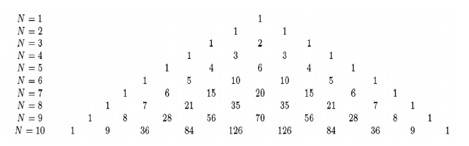
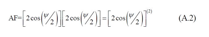
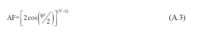
    Another case is the uniform spacing and non-uniform amplitude, an example of which is binomial arrays. The excitation coefficients of the binomial arrays for different values of N are given in FIG. A.1 [33].

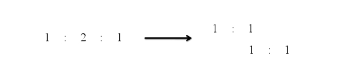
    For example in a three element array that has the current ratio of 1:2:1, we can decompose this array into two 2-element uniform arrays, as shown in FIG. A.2, with element distance d.

    So the array factor will be:

    image

    Thus, a general array factor formula for N elements array will be:

    image

    The array factor of 2-element uniform antenna array does not have minor lobes, thus, the binomial arrays will also be the same. By increasing N, for a certain d, despite the uniform case:

    The number and direction of the lobes are not changed,

    The lobe intensities are increased,

    Hence, the directivity is enhanced,

    For the same N, its lobe-width is more than that of the uniform one.

    For a given N, by increasing d:

    The number of lobes is increased,

    The directions are changed,

    The lobe-width is decreased [33-34].

참고문헌
  • 1. Bethe H. A 1944 Theory of diffraction by small holes [Phys.Rev.] Vol.66 P.163-182 google cross ref
  • 2. Yablonovitch E 1987 Inhibited spontaneous emission in solid state physics and electronics [Phys. Rev. Lett.] Vol.58 P.2059-2062 google cross ref
  • 3. John S 1987 Strong localization of photonics in certain disordered dielectric super-lattices [Phys. Rev. Lett.] Vol.58 P.2486-2489 google cross ref
  • 4. Painter O, Lee R. K, Scherer A, Yariv A, O’Brien J. D, Dapkus P. D, Kim I 1999 Two-dimensional photonic band-gap defect mode laser [Science] Vol.284 P.1819-1821 google cross ref
  • 5. Joannopoulos J. D, Villeneuve P. R, Fan S 1997 Photonic crystals: putting a new twist on light [Nature] Vol.386 P.143-149 google cross ref
  • 6. Leung K. M, Liu Y. F 1990 Full vector wave calculation of photonic band structure in face-centered-cubic dielectric media [Phys. Rev. Lett.] Vol.65 P.2646-2649 google cross ref
  • 7. Guida G, Delustrac A, Priou A 2003 An introduction to photonic band-gap (PBG) materials [PIER] Vol.41 P.1-20 google cross ref
  • 8. Zho Z.-H, Ye W.-M, Ji J.-R, Yuan X.-D, Zen C 2007 Enhanced transmission and directional emission via coupled resonator optical waveguides [Appl. Phys. B] Vol.86 P.327-331 google cross ref
  • 9. Pajewski L, Rinaldi L, Schettini G 2008 Enhancement of directivity using 2D electromagnetic crystals near the band-gap edge: a full-wave approach [PIER] Vol.80 P.179-196 google cross ref
  • 10. Liang W. Y, Dong J. W, Wang H. Z 2007 Directional emitter and beam splitter based on self collimation effect [Opt. Express] Vol.15 P.1234-1239 google cross ref
  • 11. Kurt H 2008 Theoretical study of directional emission enhancement from photonic crystal waveguides with tapered exits [IEEE Photonics Technol. Lett.] Vol.20 P.1682-1684 google cross ref
  • 12. Chung K. B 2008 Properties of surface modes used for directional emission from photonic crystal waveguides [J.Opt. Soc. Korea] Vol.12 P.7-12 google cross ref
  • 13. Chung K. B 2008 Effects of surface termination on directional emission from photonic crystal waveguides [J. Opt. Soc.Korea] Vol.12 P.13-18 google cross ref
  • 14. Kim S, Lim Y, Park J, Lee B 2010 Bundle beaming from multiple subwavelength slits surrounded by dielectric surface gratings [IEEE J. Lightwave Technol.] Vol.28 P.2023-2029 google cross ref
  • 15. Lee B, Kim S, Kim H, Lim Y 2010 The use of plasmonics in light beaming and focusing [Prog. in Quantum Electron.] Vol.34 P.47-87 google cross ref
  • 16. Kim H, Park J, Lee B 2009 Tunable directional beaming from subwavelength metal slits with metal-dielectric composite surface gratings [Opt. Lett.] Vol.34 P.2569-2571 google cross ref
  • 17. Kim S, Kim H, Lim Y, Lee B 2007 Off-axis directional beaming of optical field diffracted by a single subwavelength metal slit with asymmetric dielectric surface gratings [Appl. Phys. Lett.] Vol.90 P.051113 google cross ref
  • 18. Kramper P, Agio M, Soukoulis C. M, Birner A, Muller F, Wehrspohn R. B, Gosele U, Sandoghar V 2004 Highly directional emission from photonic crystal waveguides of sub-wavelength width [Phys. Rev. Lett.] Vol.92 P.113903 google cross ref
  • 19. Moreno E, Garcia F. J, Martin-Moreno L 2004 Enhanced transmission and beaming of light via photonic crystal surface modes [Phys. Rev. B] Vol.69 P.121402-121404 google cross ref
  • 20. Morrison S. K, Kivshar Y. S 2005 Engineering of directional emission from photonic crystal waveguides [Appl. Phys. Lett.] Vol.86 P.081110 google cross ref
  • 21. Bulu I, Caglayan H, Ozbay E 2005 Beaming of light and enhanced transmission via surface modes of photonic crystals [Opt. Lett.] Vol.30 P.3078-3080 google cross ref
  • 22. Chen C. C, Pertsch T, Iliev R, Lederer F, Tunnermann A 2006 Directional emission from photonic crystal waveguides [Opt. Express] Vol.14 P.2423-2428 google cross ref
  • 23. Guven K, Ozbay E 2007 Directivity enhancement and deflection of the beam emitted from a photonic crystal waveguide via defect coupling [Opt. Express] Vol.15 P.14973-14978 google cross ref
  • 24. Zhang Y, Zhang Y, Li B 2007 Highly efficient directional emission from photonic crystal waveguides for coupling of freely propagated terahertz waves into Si slab waveguides [Opt. Express] Vol.15 P.9281-9286 google cross ref
  • 25. Li Z, Aydin K, Ozbay E 2007 Highly directional emission for photonic crystals with a wide bandwidth [Appl. Phys.Lett.] Vol.91 P.121105 google cross ref
  • 26. Yariv A, Xu Y, Lee R. K, Scherer A 1999 Coupled resonator optical waveguide: a proposal and analysis [Opt.Lett.] Vol.24 P.711-713 google cross ref
  • 27. Oliver S, Smith C, Rattier M, Benisty H, Weisbuch C, Krauss T, Houdre R, Oesterle U 2001 Mini-band transmission in a photonic crystal coupled resonator optical waveguide [Opt. Lett.] Vol.26 P.1019-1021 google cross ref
  • 28. Bayindir M, Temelkuran B, Ozbay E 2000 Tight binding description of the coupled defect modes in three dimensional photonic crystals [Phys. Rev. Lett.] Vol.84 P.2140-2143 google cross ref
  • 29. Happ T. D, Kamp M, Forchel A, Gentner J, Goldstein L 2003 Two dimensional photonic crystal coupled defect laser diode [Appl. Phys. Lett.] Vol.82 P.4-6 google cross ref
  • 30. Ares F, Franceschetti G, Rodriguez J. A 2008 A simple alternative for beam reconfiguration of array antennas [PIER] Vol.88 P.227-240 google cross ref
  • 31. Zhou H. J, Sun B. H, Li J. F, Lin Q. Z 2009 Efficient optimization and realization of a shaped beam planar array for very large array application [PIER] Vol.86 P.1-10 google cross ref
  • 32. Yang S. W, Chen Y. K, Nie Z. P 2009 Simulation of time modulated linear antenna arrays using the FDTD method [PIER] Vol.98 P.175-190 google cross ref
  • 33. Balanis C. A 2005 Antenna Theory: Analysis and Design google
  • 34. Jordan E. C, Balmain K. G 1968 Electromagnetic Waves and Radiating Systems google
OAK XML 통계
이미지 / 테이블
  • [ FIG. 1. ]  (a) Radiative resonator excitation point CROW and radiative resonator and (b) the polar pattern of the radiative resonator in the azimuthal plane normalized to its peak.
    (a) Radiative resonator excitation point CROW and radiative resonator and (b) the polar pattern of the radiative resonator in the azimuthal plane normalized to its peak.
  • [ FIG. 2. ]  (a) The structure for derivation of the resonant frequencies of the resonator and (b) discrete Fourier transform (DFT) of the waveguide input and output with and without resonator near it.
    (a) The structure for derivation of the resonant frequencies of the resonator and (b) discrete Fourier transform (DFT) of the waveguide input and output with and without resonator near it.
  • [ FIG. 3. ]  A photonic crystal radiative array with radiative elements number of N=3 and elements distance of d=6a.
    A photonic crystal radiative array with radiative elements number of N=3 and elements distance of d=6a.
  • [ FIG. 4. ]  The optical field distribution of a 4-element radiative array with elements distance d=6a for (a) uniform excitation and (b) binomial excitation
    The optical field distribution of a 4-element radiative array with elements distance d=6a for (a) uniform excitation and (b) binomial excitation
  • [ FIG. A.1-1. ]  The excitation coefficients of the binomial arrays fordifferent numbers of array elements [33].
    The excitation coefficients of the binomial arrays fordifferent numbers of array elements [33].
  • [ FIG. A.2-1. ]  Decomposition of the three element binomial arrayinto two 2-element uniform arrays.
    Decomposition of the three element binomial arrayinto two 2-element uniform arrays.
(우)06579 서울시 서초구 반포대로 201(반포동)
Tel. 02-537-6389 | Fax. 02-590-0571 | 문의 : oak2014@korea.kr
Copyright(c) National Library of Korea. All rights reserved.