Photonic crystals (PCs) are periodic dielectric structures which under certain conditions prohibit the propagation of electromagnetic waves within certain frequency bands. This phenomenon provides the ability of guiding and manipulating the flow of light [1, 2]. PCs can be periodic in one, two or three dimensions. Slab PCs are periodic in two dimensions and have a finite thickness in the other dimension.
PCs can be used to design passive, active and nonlinear optical devices. Waveguides, filters, resonators, lasers, logical gates, etc. [3-8] can be implemented using PCs. Waveguides are realized by introducing a line defect in the PC structure[9]. The most popular method for creating a waveguide for TE modes is to remove a row of holes in a triangular lattice of air holes (which are etched in a dielectric slab). The resultant waveguide is often referred to as a “W1” waveguide.It is worth mentioning that in the same manner, sharp bends and branches can be created in PCs. The quality of optical bends and junctions are very important for many integrated optical circuits. The unwanted reflection from bends and branches can be a nuisance in many instances. Low reflection (high transmittance) devices are required for large scale integrated optical circuits. Various methods have been proposed in the literature to improve the quality of the bends [10-14], Y-junctions and splitters [15-20]. Among the methods proposed to achieve higher transmission ratios, the most effective method is to modify the structure of the waveguide in the vicinity of the discontinuity. It can be done by introducing new holes [13-14] or by changing the radii of the holes in that region. Due to the complexity of the equations governing PC behavior, analytic optimization of PC structures is very difficult and in some instances almost impossible. Numerical optimization methods are usually used for this purpose. Using optimization techniques a wideband photonic crystal Y-splitter is proposed in this paper. The rest of the paper is organized as follows: In Section 2 we describe the numerical aspects of the work. Section 3 is devoted to the optimization of a Y-junction and consequently a Y-splitter for increasing the bandwidth. Section 4 presents the simulation results regarding the proposed structures,and the final section is devoted to the conclusions.
Different slab materials can be used for creating PCs, among them GaAs and silicon are the most frequently used materials.The refractive index of GaAs, which is used in our simulations, is about 3.4 for wavelengths around 1550 nm.In our designs a photonic crystal slab with a triangular pattern of circular holes is assumed. It can provide a considerable bandgap and can easily be fabricated using integrated circuit manufacturing technology. Assuming that “
It is shown that in order to reduce the computational process, the slab structure can be modeled by a 2D structure of infinite height with an effective index [10-11], [14], [20-25]. In [21] a detailed study regarding the replacement of 3D analysis with 2D analysis has been made. It is shown that the 3D FDTD simulation results produce almost the same results as its 2D effective index approximation. The simplest method for calculation of the effective index is to compare the band diagrams of the 3D PC slab and the equivalent infinite 2D PC. The effective index of the 2D PC is chosen such that its band diagram approximately matches the band diagram of the 3D slab below the light cone. In our simulations we chose an effective index equal to 2.76. The same value has been used in [10-11], [20].Since the Y-splitter is not a straight waveguide, there always exists a vertical loss at the region where the propagation vector is changed (and the leaky modes can be excited).The mentioned loss cannot be modeled using the 2D effective index method. Although the vertical loss usually [10-11]does not create a considerable difference in the results but to be precise the transmittance notion in this paper incorporates the mentioned leakage.
The FDTD area is surrounded by a perfectly matched layer (PML) of thickness “
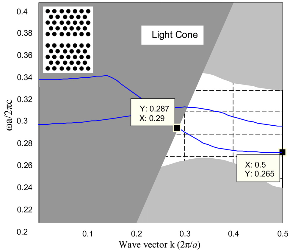
Using the plane wave expansion (PWE) method, it can be easily seen that the PC slab used in our simulations has a bandgap from 0.260 (
As it can be seen, the waveguide associated with the diagram shown in Fig. 1 has a single mode bandwidth between 0.265 (
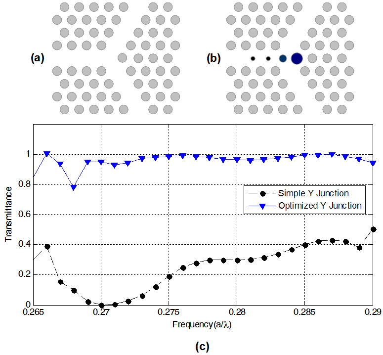
The simplest geometry which can be used as a branch is shown in Fig. 2a. The corresponding PC is the commonly used 2D triangular lattice of circular holes embedded in a 0.6a thick GaAs slab. By removing two columns of air holes adjacent to a W1 waveguide, a 120-degree Y-branch can be created. An ideal branch should divide the incident light beam to two distinct sections; with 50% of the incident power
traveling in each direction (100% transmission ratio). Zero reflection is expected for the entire frequency range of the corresponding W1 waveguide; therefore the bandwidth used in this paper is normalized to the single-mode region of the W1 waveguide. For the branch shown in Fig. 2a, FDTD simulation results show that the maximum transmission coefficient does not exceed 48% (24% for each arm), which is equal to a 52% reflection of the incident power. The high reflection ratio makes the mentioned structure unsuitable for many integrated optic applications. By introducing modifications to the structure of the branch the transmission spectrum can be improved [16-17], [19]. There have been some detailed topologies reported in the literature which enhance the bandwidth [26, 27]. The structure implemented in [26] provides a bandwidth of more than 100 nm. However; the structures presented in [26, 27] are hard to define, manufacture and reproduce. Some holes are not circular; some are merged together; while for our design, the each hole is circular and has a defined radius.
Our proposed Y-junction structure is shown in Fig. 2b.In comparison to the previous branch, three additional holes are introduced to the structure and the radius of one hole is also increased. An optimization algorithm (using FDTD method for evaluating the structures) is used to calculate the optimum values for the holes. The method used for the optimization of bandwidth is taken from [3]. It uses a neural network optimization engine to find the optimum values for the variables. An evaluation section calculates the transmittance curve for each set of input variables. The next block calculates the percentage of the transmittance curve which is more than 0.9. The obtained number is considered as the bandwidth. In other words, instead of using the conventional 3 dB criteria for calculating the bandwidth,we use the 90% limit which is approximately equal to 0.45 dB. The algorithm mentioned finds the input variable set that maximizes the bandwidth. In order to optimize the junction, the central junction’s hole’s radius is chosen as Var2, The right side hole’s radius is considered to be Var1 and the remaining two left-side holes are assigned an identical radius denoted by Var3. After the optimization phase,the optimum variables are obtained as: Var1=0.4a, Var2=0.31a and Var3=0.12a. Fig. 2c shows the transmittance curve(summation of the two output arms) for the proposed junction in comparison to a simple junction. It is seen that a bandwidth equal to 94% is obtained.
Yang et. al. used a triangular lattice of dielectric rods to design a Y-Branch [17]. They showed that the Y-branch can be treated as a cavity that couples with the input and output waveguides. In order to enhance the transmittance,additional rods are added to the junction area and the corner rods are displaced. The movement of the corner rods can increase the volume of the cavity and make the cavity mode resonant with the waveguide modes. It is shown in [17]that using the coupled mode theory the reflection coefficient can be expressed as (1).
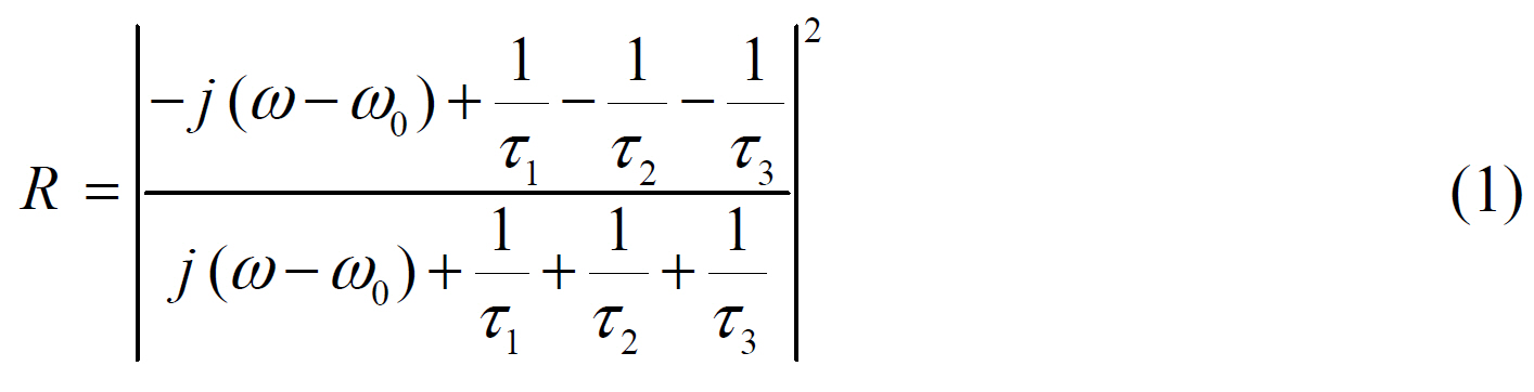
Where, ω0 is the resonance frequency, τi is the time constant regarding the amplitude decay of the resonance into the ith port. It is seen that if the (2) is satisfied, the reflection will be zero for ω = ω0.
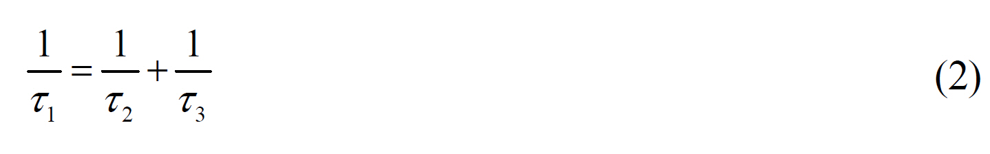
We already know that due to symmetry τ2 =τ3; therefore the condition mentioned can be simplified as: τ2 =2τ1. It means that the decay rate of resonance to the output ports should be half the decay rate of resonance to the input port. In a simple Y-junction all of the three time constants are equal. The tapered structure of the holes inserted in our proposed design, improves the coupling strength between the resonator and the input waveguide. It results in the reduction of τ1. If the tapering is designed so that τ1 is reduced to half τ2, then the zero reflection condition can be satisfied. Numerical optimization is used to design such a tapering. In [17] two rods are placed at the output waveguides to reduce the coupling strength of the output waveguides (to increase τ2), while we decrease τ1 to obtain similar results.
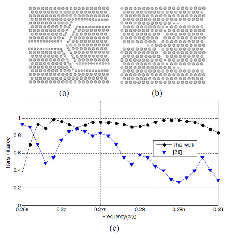
In order to create a PC Y-splitter the aforementioned optimized Y-junction and two additional optimized PC 60-degree bends are combined. Figure 3 depicts the Y-splitter structure proposed in this paper and the recent bi-periodic Y-splitter proposed in [20]. Five additional holes have been added to the structure of a conventional PC bend to maximize the transmission bandwidth [14]. The radii of four of these holes are 0.11a and the other’s radius is 0.19
For the bend embedded in Fig. 3b, ΓJ denotes the 0-degree and equivalently 60-degree directions. When light passes through the bend, it can be assumed that, first it transmits along the 0-degree direction then turns in to the transient modes of 30-degree and finally turns back to the 60-degree direction. Assuming that ΓX represents the direction at the bend, namely 30-degrees, it can be easily shown that the mentioned structure has one guiding mode in the ΓJ direction and two guiding modes in the ΓX direction [14]. Therefore the coupling of energy between the modes is not perfect.It results in a higher reflection or equally a lower transmission from the bend. Modifying the topology of the waveguide in the vicinity of the bend can change the profile of the guiding modes in ΓX direction. In [14], some additional
holes with identical sizes are introduced in the structure to move one of the ΓX modes out of the band and enhance the coupling. It is a well-known principle that gradual change or tapering in the vicinity of discontinuity can lead to the reduction of reflection. It is expected that if the radii of the holes change in a gradual manner a lower reflection coefficient can be obtained. The optimization process of the previous section confirms the same concept.
The transmission spectrum of the structures shown in Fig. 3a and Fig. 3b are depicted in Fig. 3c. As it can be seen, regarding the structure in Fig. 3a, for only a small portion of the available W1 waveguide bandwidth, the transmission ratio exceeds 0.8. The transmittance of the splitter proposed in this paper is also shown in Fig. 3c, whose normalized bandwidth is 79%, which is a considerable improvement in comparison with the structure reported in [20]. Furthermore;the proposed structure has the benefit of simplicity in regard to the bi-periodic structure in Fig. 3a. The small holes in the mentioned figure are very close to each other. A slight manufacturing error might cause them to join together;which results in the total failure of the structure.
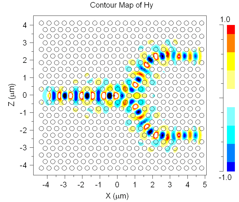
To have a better visual perception of the proposed Y-Splitter,the time domain simulation results regarding the amplitude of the vertical component of the magnetic field for an input wavelength equal to 1550 nm has been presented in Fig. 4. As can be seen in this figure, the incident power is neatly divided in to two distinct sections.
We have determined the normalized holes’ radii as:0.4
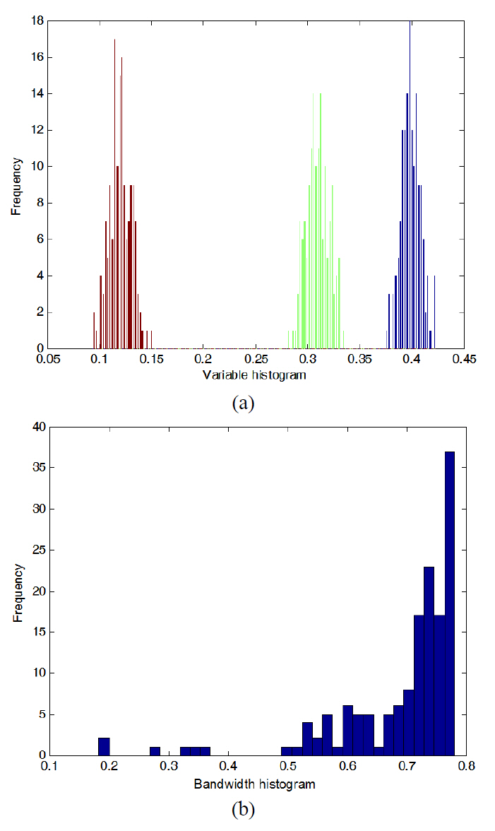
from the optimum values. Some holes might become bigger while the others become smaller than the desired value.These variations normally have a Gaussian distribution. Here each hole’s radius is independently assumed to have a variance of 4 nm. A set of 150 statistically different samples are produced, in which each variable has a Gaussian variation from the desired values. The histogram of the mentioned set is shown in Fig. 5a.
As it is seen, the first variable varies independently in the 0.38
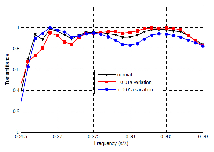
What we considered before was the worst case scenario;however in reality the hole sizes usually vary in the same manner. They either become a bit wider or narrower. In order to simulate the mentioned effect, we first assume that all holes become 0.01a larger (0.41
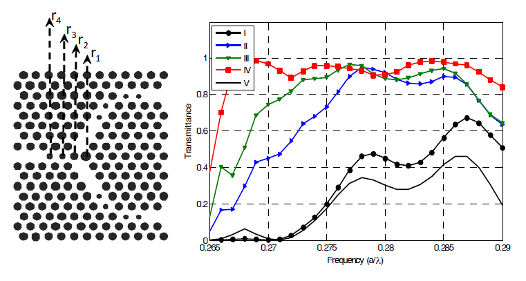
In order to investigate how the three added holes improve
the transmission spectrum, the transmittance curves for different configurations are presented in Fig. 7. The notation r1-r4
specifies the radii of the holes. Removing a hole can be done by assigning a zero radius to it. For case (V) in Fig. 7 the radius of the junction hole (r1) is assumed 0.3a,as the rest of lattice and the rest of additional holes do not exist. A simple junction is obtained in this case. As can be seen in Fig. 7 the worst transmission happens for the simple junction. When the radius of junction hole is increased from 0.3
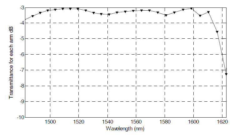
Finally in Fig. 8 the transmittance curve is depicted in dB scale versus wavelength to provide a more physical insight on the performance of the Y-splitter.
A PC Y-splitter for TE modes was proposed in this paper.FDTD method was used to analyze the proposed structure.Simulation results confirm that in comparison to the most recent structures reported in literature, the proposed Y-splitter provides an improved transmittance and bandwidth, while it has a much simpler design. For a bandwidth more than 120 nm the transmittance curve has less than 0.5 dB fluctuations.


![(a) The bi-periodic structure proposed in [20] (b) Thestructure proposed in this paper (c) The transmittance for thestructures in Fig. 3a and Fig. 3b.](http://oak.go.kr/repository/journal/10731/E1OSAB_2011_v15n3_283_f003.jpg)