Quasi-phase matching (QPM) devices are widely used because phase matching is always possible between interaction waves by reversing the sign of nonlinear coefficients at every coherence length . QPM has the advantage that the largest nonlinear coefficient can be utilized for obtaining high conversion efficiency. Moreover, phase matching within the transparent region of a nonlinear crystal is achieved easily and spatial walk-off can be eliminated by propagating light along the optic axis of a birefringent medium [1].Possessing spontaneous polarizations which can be reversed by an external electric field, ferroelectric crystals have been widely used for fabricating QPM devices. There are many kinds of ferroelectric crystals such as LiTaO3, LiNbO3, KTiOPO4 (KTP) and so on. Above all, LiNbO3 is the most attractive ferroelectric crystal due to its large nonlinear coefficient (d33 = 27 pm/V) [2].
Fabrication of periodically poled LiNbO3 (PPLN) has been developed since the 1980s [3, 4]. In particular, a high electric field poling method at room temperature made it possible to fabricate periodically poled bulk devices [5, 6]. Additional techniques such as corona discharging [7], temperature elevation [8], UV lightening [9] and back-switched voltage waveform [10] were demonstrated to manufacture high-quality PPLN with short-pitch QPM periods. Real-time monitoring of polarization reversal during electric field poling also assists to produce the high-quality PPLN because it is possible to observe domain structures nondestructively. Therefore,real-time domain visualization has been broadly used in many research groups [11, 12].
In this work, we introduced a new poling method which was the negative multiple pulses poling (NMP) method combined with our real-time visualization system to fabricate uniform PPLNs in periodicity. We applied negative incubation voltage (-4.5 kV) before the poling voltage, then the pulse was repeated until the end of the poling process during the real-time monitoring of polarization reversal. The poling quality between NMP and other two conventional pulse poling methods was compared by showing microscope images on +z and ?z surfaces of PPLN samples and analyzing the duty ratios by utilizing far-field diffraction patterns.
II. EXPERIMENTS AND DISCUSSION
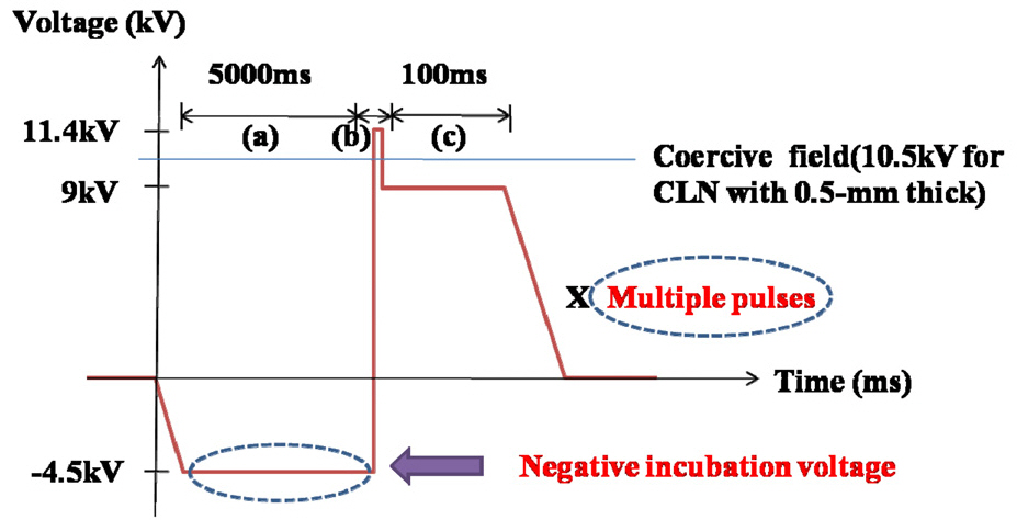
We used a z-cut congruent LiNbO3 (cLN) wafer 0.5-mmthick and 3-inch diameter (Crystal Technology Inc). Liquid electrodes using photoresist patterns (Clariant, AZ5214E)were formed on the +z surface of the cLN wafer. The pattern thickness was 1.2 ㎛ and the QPM period was 12.9 ㎛. For polarization reversals, high DC voltage was applied to the cLN crystal with the waveform as shown in Fig. 1. The voltage waveform consisted of 3 parts: incubation(a), polarization reversal (poling) (b), and stabilization (c).The conventional incubation voltage of cLN was about 9 kV [13], which had the role of preventing crystal damage from a sudden increase in the poling voltage. However,our incubation voltage in Fig. 1 (a) was -4.5 kV which was not only half of the conventional value but also a negative pulse. The reason is that it was observed that the polarization reversals occurred even in the photoresist part when a long pulse was applied for poling. It means that the domain merging which can obstruct the formation of periodic domain structures can occur due to the long poling time. Therefore, we ensured that photoresist was not a perfect insulator any more during the long poling time. If photoresist is considered as a capacitor, the negative incubation voltage (-4.5 kV) can support longer time than the conventional incubation voltage (9 kV) for charging up the photoresist.Accordingly, if the waveform with the negative incubation voltage shown as in Fig. 1 is repeated during the whole process, domain merging can be reduced.
In general the incubation voltage was determined by not only the back-poling field but also the difference between
the incubation voltage and the poling voltage. Because the incubation voltage should not create polarization reversals,so it is higher than the back-poling voltage which can invert polarization switch back to the original polarization state. The reported back-poling field of cLN is about -16 kV/mm [14]. Furthermore, a large difference between the incubation and poling voltage can cause crystal damage.Therefore, we applied the incubation voltage of -4.5 kV for 5 seconds. In the case of cLN, coercive field for inverting polarizations is about 21 kV/mm [14]. The poling voltage as shown in Fig. 1 (b) reversing the spontaneous polarization of cLN should be higher than coercive field because nucleation density depends on electric field strength. The applied poling voltage was 11.4 kV and the poling charge(Q) was estimated by the hysteresis loop of cLN (Q ~ PsA, Ps = spontaneous polarization of cLN (~ 78 μC/cm2), A = poled area) [15]. The calculated poling charge was 73.1 μC and the poling current was set to 2.1 mA, so the estimated poling time was 34.8 ms.
After polarization reversal, the reversed domain is not stable for some moments thus a sudden voltage drop can be induced by back-switching. To protect against back-switching a stabilization voltage should exist after the poling as shown in Fig. 1 (c). It was known that the stabilization time needed to be longer than ~50 ms for maintaining the inverted polarizations after polarization reversal [15].Therefore, we applied 9 kV of stabilization voltage for a long enough time such as 100 ms. The designed waveform as presented in Fig. 1 was applied to the cLN crystal repeatedly by changing the poling time (Fig. 1(b) part)using measured voltages in oscilloscope and real-time visualization images.
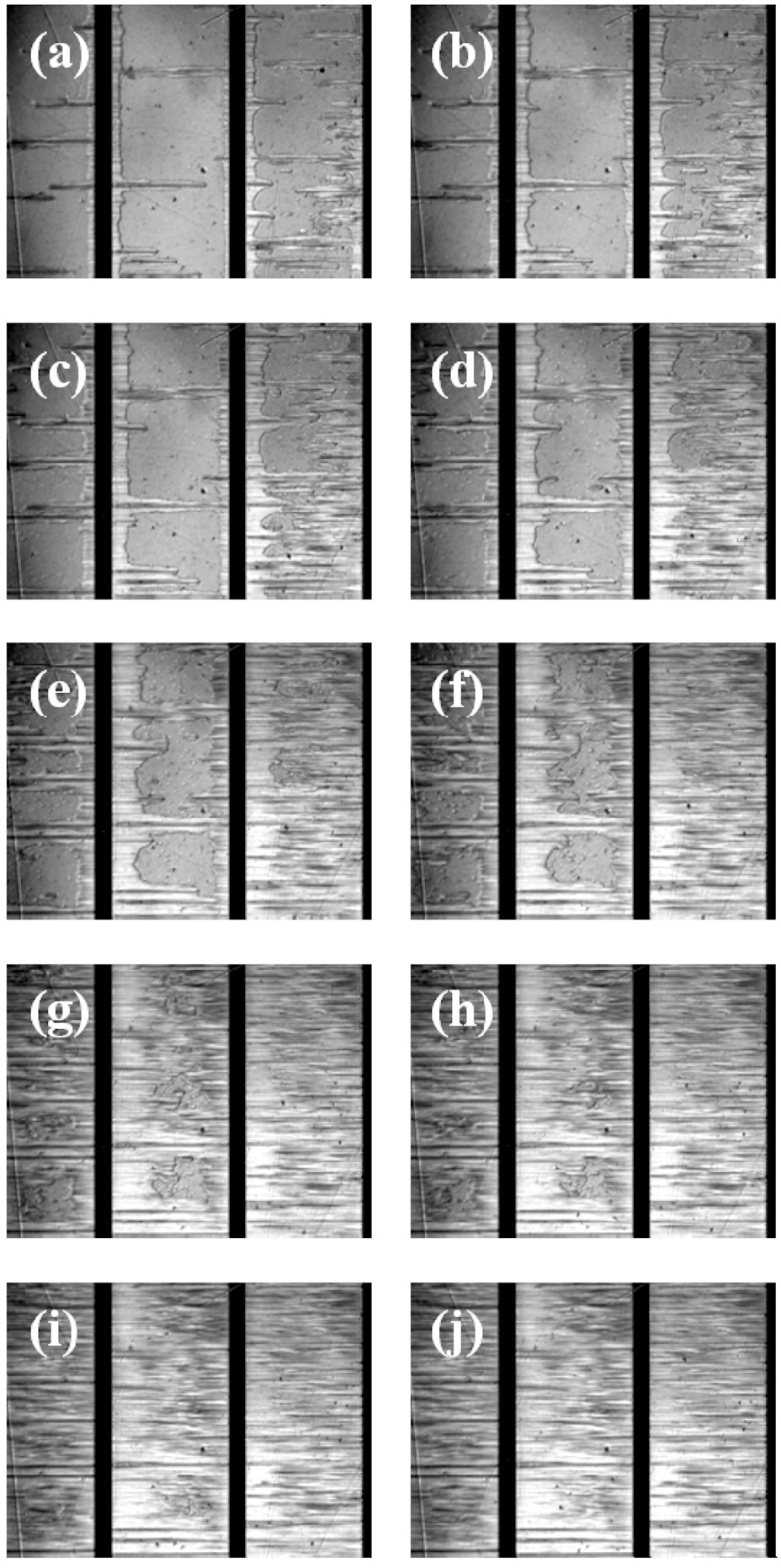
Fig. 2 shows the expansion of the poled area in the +z surface of cLN during electric field poling by the real-time visualization system. Because of the electro-optic effect on the domain boundary one can see the contrast of the domain images [16]. The grey color of the images represented the patterned area on the +z side and the black color was the non-patterned area. The color difference between the patterned and non-patterned surfaces was due to its reflectivity. Most of the domain nucleation had occurred at the edges of the patterned area and the domains created had propagated along patterned areas as presented in Fig. 2. When all patterned areas had been poled by checking the real-time images, the poling process was terminated.
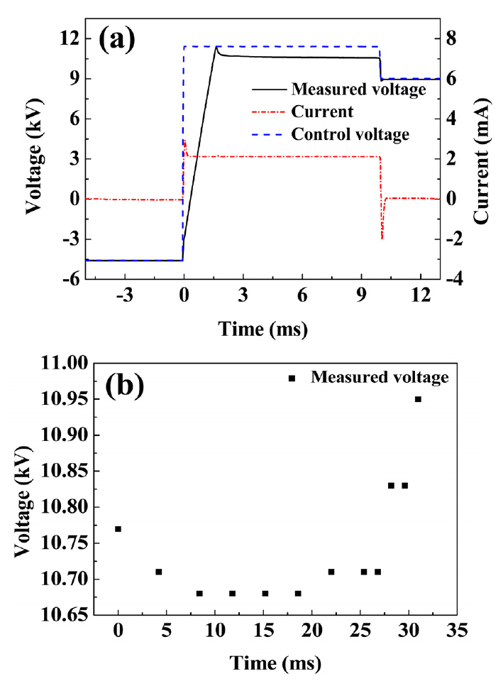
The measured voltage is also one of the key parameters for manufacturing high quality PPLN. Figure 3 (a) shows the oscilloscope data during the first poling time of 10 ms.Measured current was 2.1 mA. The high-voltage amplifier(Trek 30/20) had a current limit thus the trend of the control voltage was not the same as that of the measured voltage during the poling. Figure 3 (b) showed the variation of the poling voltages measured by each pulse during the electric poling. After the nucleation voltage (10.77 kV)was applied, the voltage was dropped to 10.71 kV then kept constant for 10 ms. The constant voltage, which was
lower than the nucleation voltage, means that the polarization reversal was carried out without domain merging. After 18.6 ms of the whole poling process, the poling voltage began to increase due to the creation of the inverted polarization under photoresist. The open ratio of the photoresistpatterned on cLN was 0.2 (electrode width of 2.6 ㎛), so some voltage increase was needed for making the PPLN with duty ratio of ideal value of 0.5. Viewing the realtime visualization images and comparing with the calculated poling time, we determined we have to stop the poling process at 10.95 kV. The measured total poling time was
31 ms which was a little bit smaller than the estimated poling time of 34.8 ms.
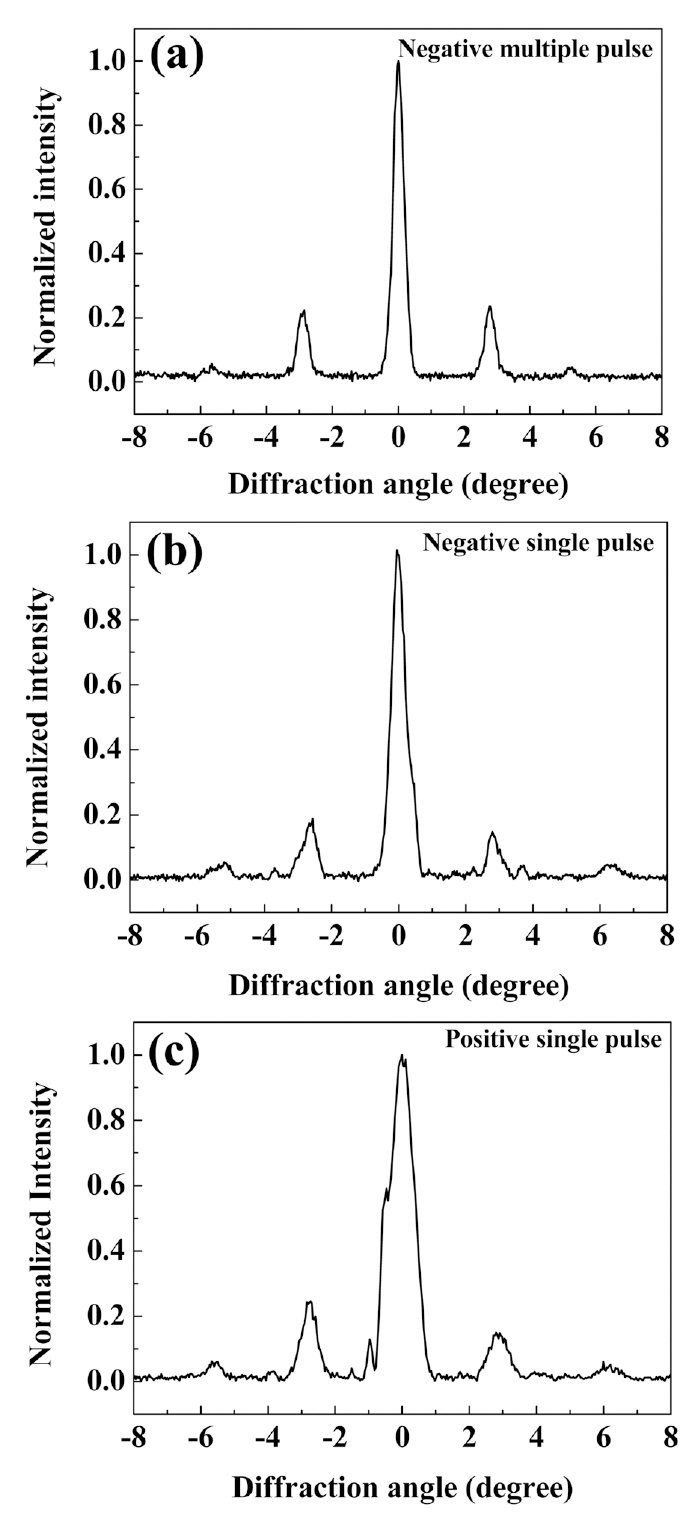
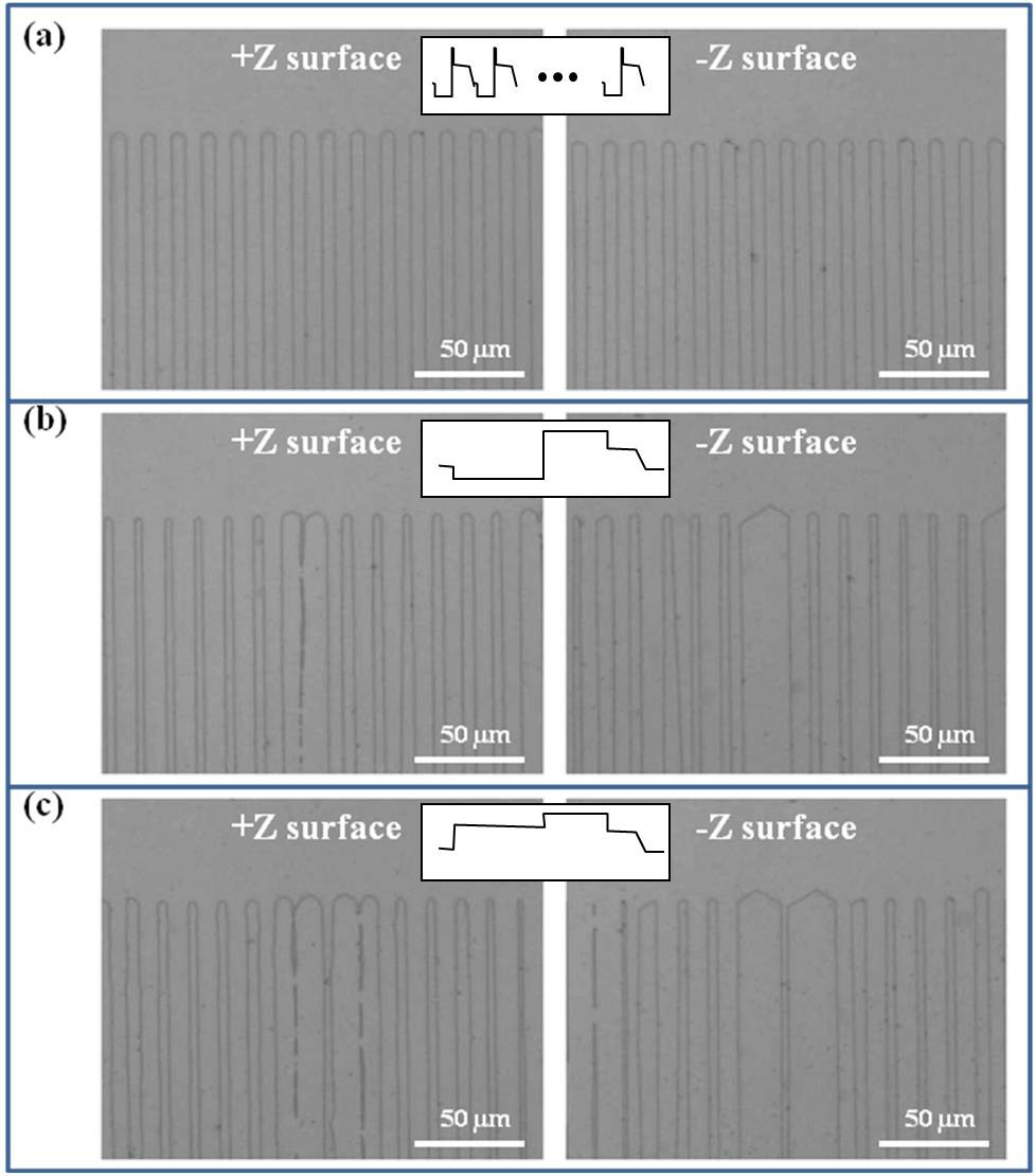
For comparing the poling quality between NMP method and other conventional pulse poling methods, we performed the electric field poling with two different pulse poling methods. One is the positive single pulse poling (PSP) by conventional pulse form with the incubation voltage of 9 kV. The other is the negative single pulse poling (NSP)with the incubation pulse of -4.5 kV. After finishing the poling with three different methods, the poling quality with three samples was checked by observing the etched microscopic images and analyzing by far-field diffraction patterns. First of all, we etched the three samples in a HF:HNO3 (1:2) solution and observed the domain structures on +z and ?z surfaces. Fig. 4 (a) with NMP method showed the uniform periodic domain structures on both +z and -z side. However, Fig. 4 (b) and (c) obtained by NSP and PSP, respectively, showed the domain merging and non-periodic poled domains.
Although we knew just from observing just microscopic etched images that the sample fabricated by NMP method had better poling quality that was not sufficient to perform quantitative analysis of the device quality. Therefore, we applied far-field diffraction pattern analysis which was introduced by Cha and co-authors [17] to evaluate the poling quality, especially duty ratio which is the ratio of the poled (un-poled) domain width divided by the grating
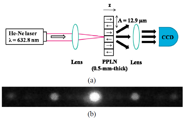
period. SHG spectrum presents overall nonlinear performance of QPM device, but it is mathematically equivalent to the far-field diffraction pattern and experimentally proved by Refs. 18-19. As shown in Fig. 5 (a), He-Ne laser at the wavelength of 633 nm passed through the poled sample along the z-direction of the crystal and then the light was diffracted by the internal field variation of PPLN shown by Fig. 5 (b). It was known that the intensity ratio between the first and second diffraction orders presented as [18-19]
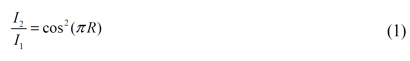
where
diffraction order, respectively, and R is the duty ratio. The diffraction intensities about three samples were measured as shown in Fig. 6. The duty ratio was averaged in the poled area within the beam diameter. The focusing diameter was 75 ㎛ of full width half maximum and QPM period was 12.9 ㎛, so 5 or 6 grating periods were participated in one focusing area of the sample.
We measured the intensities of first and second orders 20 times while changing the poled areas and evaluated the duty ratio using Eq. (1) and obtained the standard deviations for each sample. The results were summarized in Table 1.The cLN sample with NMP had the highest R among
[TABLE 1.] Duty ratios (R) and standard deviations (SD)among the three samples (NMP, NSP and PSP)
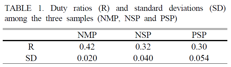
Duty ratios (R) and standard deviations (SD)among the three samples (NMP, NSP and PSP)
three samples. Moreover, the SD was 2~3 times smaller than that of the NSP and PSP. The R of the sample obtained by NMP was still smaller than ideal duty ratio 0.5 for acquiring the highest conversion efficiency. One reason to be considered was that the poling charge was not enough. However, NMP indicated relatively low SD as distinct from NSP and PSP.
In summary, we fabricated 0.5-mm-thick PPLN with QPM period of 12.9 ㎛. For fabricating high-quality PPLN,a new NMP method was demonstrated combined with the real-time visualization system, and the variation of the measured voltages was monitored during electric field poling.Through comparing poling quality for three different ways(NMP, NSP and PSP), it was determined that the proposed NMP method gave the highest duty ratio of 0.42 and the smallest standard deviation of 0.020 by far-field diffraction pattern analysis. We expect that NMP method can be used for fabricating short-pitch QPM device with the real-time visualization system. The fabricated QPM device can be utilized for various optical applications such as optical parametric oscillator, second harmonic generation, THz generation and so on. Recently, we applied the NMP method using a metal electrode to fabricate short-pitch QPM device of 6.5㎛ for green light generation.