The applications of zinc oxide (ZnO) include thin film solar cells, piezo-electric devices, sensors, and photo detectors. ZnO thin film has attracted interest due to electronic and optical properties, such as 3.3 eV direct band gap energy, high exciton binding energy of 60 meV, and high optical transmission (above 80%) [1-3]. The advantages of ZnO thin film include easy to control electrical and optical properties through doping, and low cost. Patterning is an essential process to make a device. The fine electrodes are needed to obtain fine resolution of pixels. This is required to obtain fine device features. In recent years, device sizes have decreased following with the size of devices diminishing by degrees. A conventional wet etch process does not satisfy the requirements of nano-scale feature size due to the property of isotropy. However, the dry etching process for ZnO thin film is necessary for advanced device fabrication due to its anisotropic etching property. Dry etching has been used in the fabrication process of ZnO-based devices. Plasma-induced damage causes critical errors in optoelectronic device action. In recent years, the ZnO studies have attempted to improve material performance. However, insufficient studies are available on ZnO thin film plasma etching.
In this work, we investigated the etching characteristics of ZnO thin film and the physical effect of inert gases in an inductively coupled plasma (ICP) system. The etching characteristics of ZnO thin film were investigated, as a function of the Cl2/N2, Cl2/He,
and Cl2/Ar gas mixing ratios. The physical effect of inert gas on the thin film state was investigated using X-ray diffraction (XRD) spectroscopy. The surface morphology of ZnO thin films was determined using atomic force microscopy (AFM).
Two hundred nm-thick ZnO thin films were grown on Si substrates using atomic layer deposition. We investigated the etch rate of the ZnO thin film using Cl2-based chemistry plasma mixed with Ar, N2, and He gas. The inert gas flow rate was increased from 5 sccm to 20 sccm in Cl2 plasma. The experiment set four parameters: 20 sccm flow rate, 600 W radio-frequency (RF) power, 150 W bias power, and 2 Pa process pressure. Experiments were performed by changing a specific inert gas, whilst maintaining the other parameters at the base condition. The etch rate of the ZnO thin films was determined using a surface profiler (Alpha-Step 500; KLA Tencor, Sanjoe, Ca, USA). The physical effects on the etched ZnO thin films were determined by XRD (D8-Advance; Bruker AXS Co., Karlsruhe, Germany). The XRD equipment consisted of the line detector, monochromator,and horizontal/vertical angle goniometer. The measurement
circle diameters were 435 mm, 500 mm, 600 mm, or any intermediate value. The X-ray diffractograms were scanned over an angular range of 30-65° (2θ) with a step length of 0.02° (2θ) using Cu Kα1 radiation. The surface morphology was determined by non-contact AFM (NANO Station II; Surface Imaging Systems, Herzogenaurach, Germany). All samples were the ZnO thin film with a 1 cm × 1 cm sample size.
ZnO thin film etching experiments were performed in chlorine-based plasma. The objective of our experiment was to investigate the effect of the inert gas on ZnO thin film using Cl2 chemistry plasma.
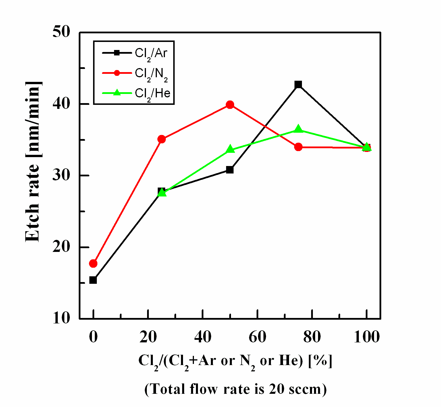
Figure 1 shows the etch rate of ZnO as a function of the inert gas content in the Cl2 plasma. Figure 1 does not show data for 100% He flow, since it was very difficult to maintain stable process pressure for the 2 Pa condition in our ICP equipment. The maximum etch rates of the ZnO thin film were 44.3, 39.9,and 37.9 nm/min at Cl2(75%)/Ar(25%), Cl2(50%)/N2(50%), and Cl2(75%)/He(25%) plasma. The chemical reactions on the ZnO thin film in Cl2 plasma were derived from the compound of ZnxCly [4-7]. The Zn-Cl compound was a volatile byproduct with a melting point of 290℃. The ion bombardment of the novel gas ions supported the chemical reaction of Cl2 by break-
ing the zinc oxide bonds. The results of the experiment indicated the noble gas induced physical etching and assisted the chemical reactions on the ZnO thin film.
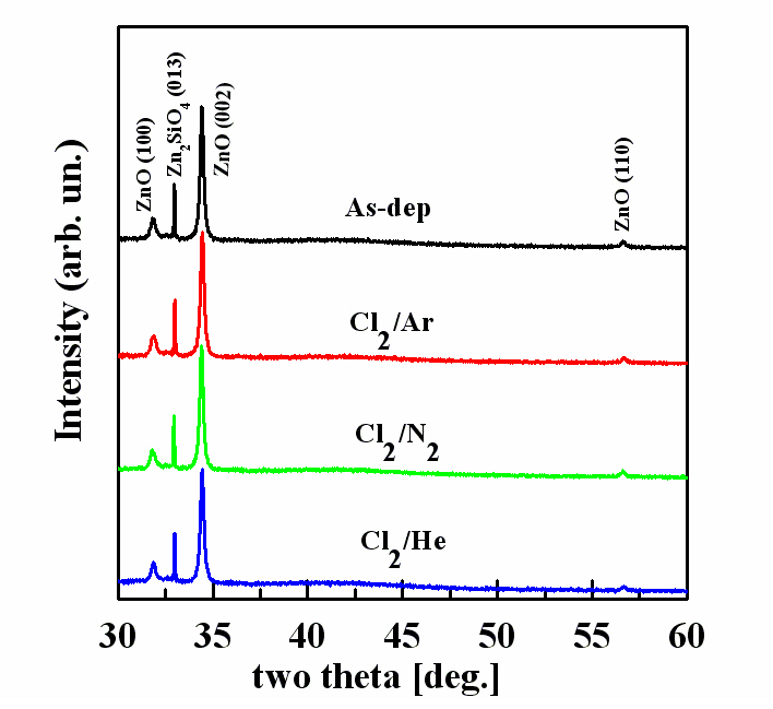
Figure 2 shows XRD 2θ patterns of the ZnO films, as a function of the Cl2/Ar, Cl2/N2, and Cl2/He gas mixing ratios and the as-deposited sample. The XRD pattern of the ZnO thin films was used to investigate the physical effects of inert gas in plasma etching of Cl2-based chemistry. The ZnO diffraction pattern was obtained in conditions that indicated a high etch rate in the gas mixture ratio. As shown in Fig. 2, the ZnO peaks detected were (002), (100), and (110). The XRD patterns for Cl2/Ar, Cl2/N2, and Cl2/He plasma were similar to that of the as-deposited sample. In addition, the (013) peak of Zn2SiO4 appeared. This can be explained by the fact that Zn2SiO4 compound was detected in the interface of the two materials by the X-rays transmitted through 200 nm of the ZnO thin film to the Si substrate. The intensity of the peaks changed only slightly. This factor shows that metal chloride compounds (ZnxCly) volatilized during the etching of the ZnO thin films and did not affect the stoichiometry of the ZnO thin films.The unchanged stoichiometry and small ion bombardment of the inert gases that flowed at 5 and 10 sccm caused the crystallinity of the ZnO thin films to maintain and inhibit the creation of other crystal orientations. However, there was a possibility of crystalline damage in the structure of the ZnO thin film.
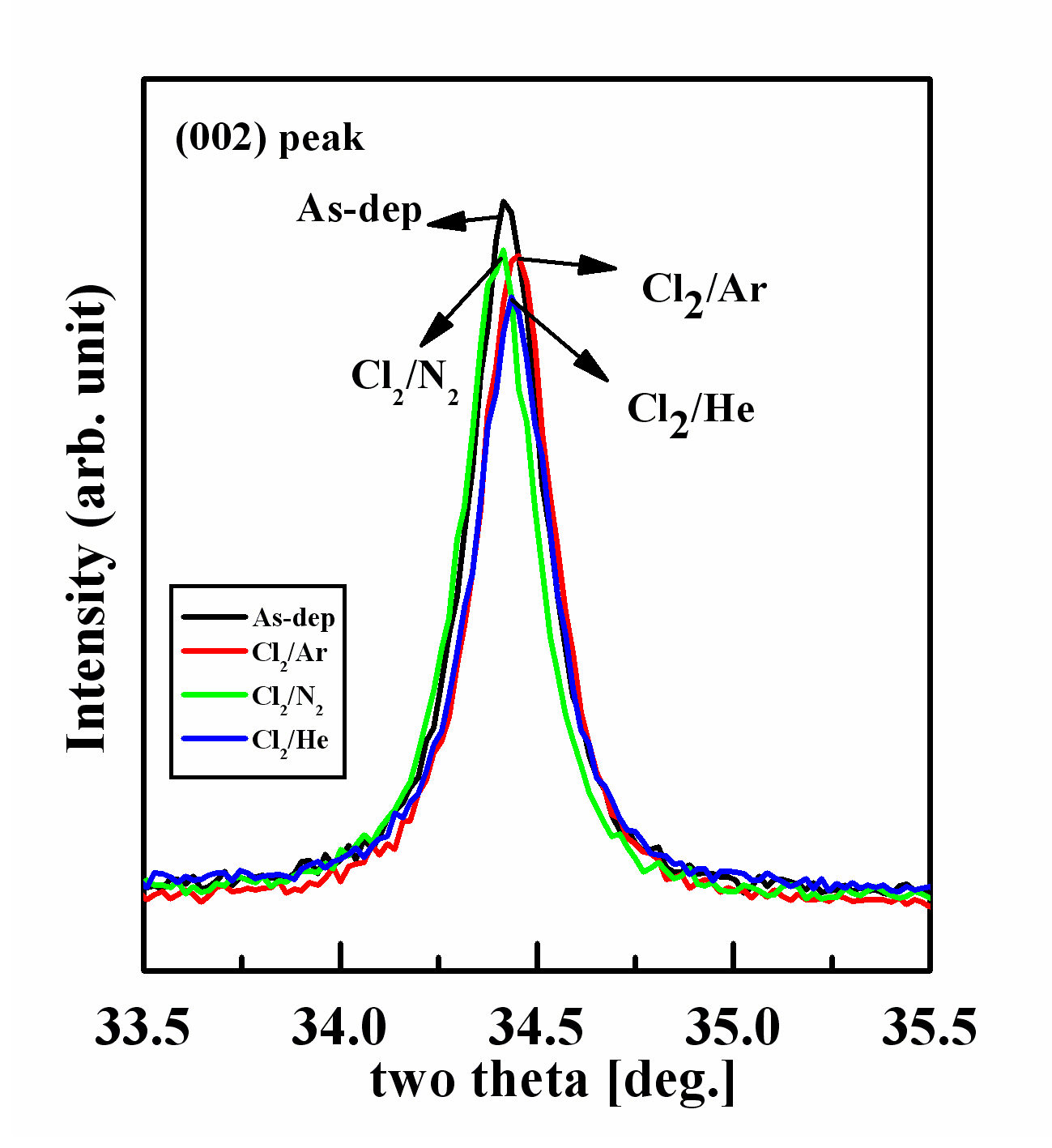
Figure 3 show the intensity of (002) peaks at each gas chemistry.The diffractogram of the as-deposition film sample shows the highest intensity in the (002) peak, while the other (002) peaks decreased in various plasma chemistry. In the Cl2/N2 and Cl2/Ar plasma chemistry, (002) peak intensity was decreased more than for the as-deposition film and peak intensity shows small difference between the Cl2/N2 and Cl2/Ar plasma. At the same time, (002) peak at the Cl2/He plasma exhibits lower intensity than the other peaks. These results allow us to assume that the Cl2/He chemistry during etching cause severe damage at the ZnO thin film surface.
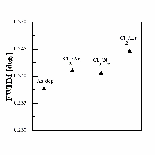
Figure 4 shows the full-width at half-maximum (FWHM) values of the (002) peak for various gas mixtures. The experiments showed that the FWHM values of the etched ZnO films are higher than those of the as-deposited films. In this case, a high FWHM value means that the crystalline structure was incomplete [8-12]. These results indicate that ion bombardment during etching damaged the crystalline structure of the ZnO thin film surface. The different gas chemistry plasmas increased the FWHM values, indicating that the ZnO thin films have damaged crystalline due to ion bombardment. Degradation of crystallinity can be explained by inert gas ion bombardment creating an unstable crystalline structure. In addition, the Zn-O bond breaking contributed to the unstable state in the ZnO thin films and degraded the crystallinity of the ZnO thin films. However, the range of fluctuation of FWHM values was too small (~0.1 θ), which means that the crystalline damage-induced plasma etching definitely existed, even though it was infinitesimal.
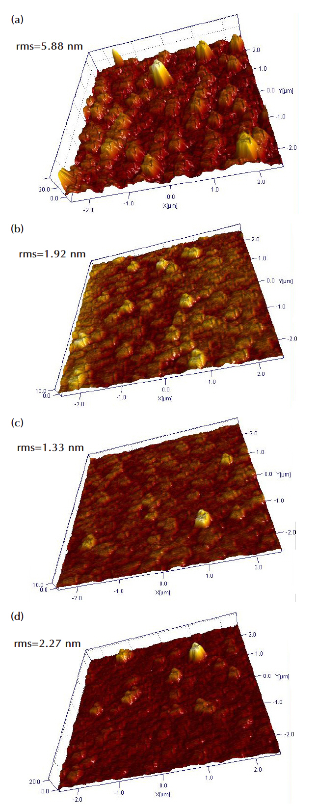
Figure 5 shows a three-dimensional (3-D) AFM image of the etched ZnO thin films in Cl2-based plasma chemistry. Figure 5(a) shows that the root mean square (RMS) roughness of the asdeposited sample was 5.88 nm. As shown in Fig. 5(b), the ZnO thin film sample using Cl2(75%)/Ar (25%) plasma exhibited 1.92 nm of RMS roughness. Figure 5(c) shows a sample with Cl2(50%)/N2(50%) chemistry that was determined by AFM to have 1.33 nm RMS roughness. Figure 5(d) shows Cl2(75%)/He(25%) plasma etching experiment, and the sample shows a decrease of 2.27 nm of RMS roughness, as shown in Fig. 5(d). The etched samples exhibited lower RMS roughness than the as-deposited sample based on the etching experiments.
We investigated the effect of inert gas additives on ZnO thin films in Cl2/Ar, Cl2/N2, and Cl2/He plasmas. The novel gas additive influenced the physical state of the ZnO thin film. The maximum etch rates were 44.3, 39.9, and 37.9 nm/min at a gas mixture of Cl2(75%)/Ar(25%), Cl2(50%)/N2(50%), and Cl2(75%)/He(25%), 600 W RF power, 150 W bias power, and 2 Pa process pressure. Oriented (002), (100), and (110) ZnO peaks were detected by XRD analysis. In addition, a (013) Zn2SiO4 peak was obtained from the XRD results. The etched samples exhibited high FWHM values at the (002) peak, indicating damage to the crystallinity. The surface roughness of the as-deposited sample was 5.88 nm in the 3-D AFM image. However, the surface roughnesses of the etched samples were lower than for the as-deposited sample,such as 1.92 nm at Cl2/Ar chemistry, 1.33 nm at Cl2/N2 chemistry,and 2.27 nm at Cl2/He chemistry. In addition, the He gas showed high roughness and a high FWHM value from XRD and AFM analysis results. We assume that the He ions were lighter than the other inert gas ions. Heavy ions were not accelerated as rapidly as light ions. The small He ion can permeate the ZnO thin film lattice. We assume that ion bombardment of the He ions caused more crystalline damage, and the effect of the He gas that makes the cooling substrate and stable plasma lead to a low etch rate due to the decreasing temperature for chemical reactions.