In recent research, zinc oxide (ZnO) was shown to be suitable for optoelectronic devices such as liquid crystal displays, solar cells, sensors and piezoelectric devices. ZnO thin films have unique properties, such as a direct band gap energy of 3.3 eV,exciton binding energy of 60 meV and light transmission exceeding 80% [1-4]. Following the downsizing of the device scale, the conventional wet etching process is no longer suitable, due to the narrow line width of the devices and elaborate processing because of their isotropic properties. Problems are encountered in the wet etching process with devices of smaller size, such as the over etching phenomenon. For this reason, anisotropic plasma etching is generally used in the fabrication process. The plasma induced damage causes critical errors in the operation of optoelectronic devices. Research into the use of ZnO has rapidly accelerated over the last few decades, such as its etching mechanism,thin film deposition, defect and doping control and ZnO based devices. However, insufficient studies have been done on the damage incurred by ZnO thin films during plasma etching in the dry etching process.
In this study, we investigated the surface and crystal structure damage of ZnO thin films and measured the etch rate using an inductively coupled plasma (ICP) system. The etch rate of the ZnO thin films was investigated as a function of the gas mixing ratio. The crystal damage on the etched surface of the ZnO thin
films was investigated by X-ray diffraction (XRD). The etched surface reaction of the ZnO thin films were obtained to roughness by atomic force microscopy (AFM). We also determined the optical properties of the ZnO thin films by photoluminescence (PL) measurements.
In this work, ZnO thin film samples with a thickness of 200 nm were grown on quartz substrates by atomic layer deposition (ALD). The etching experiments of the ZnO thin films were performed using an ICP system. The ICP system consisted of a chamber, electrodes, gas supply, mass flow controller (MFC) and turbo molecular pump. We investigated the etch rate of the ZnO thin films using a Cl2 based chemistry plasma that was mixed with Ar and O2 gases. The gas mixing ratio was controlled by the MFC. The conditions of the etching experiment were a total flow rate of 20 sccm, an radio-frequency (RF) power of 600 W, a bias power of 200 W, and a process pressure of 2 Pa. The physical effects on the etched ZnO crystal were determined by XRD (D8-Advance; Bruker AXS Co., Karlsruhe, Germany) with Cu Kα1 radiation. The X-ray diffractograms were scanned over the angular range of 30-65° (2θ) with a step length of 0.02° (2θ). The surface morphology of the etched ZnO thin films was determined by AFM (NANO Station II, Surface Imaging Systems) in non-contact mode. All of the ZnO thin film bare samples were prepared with a sample size of 1 cm × 1 cm. The PL measurements were performed at room temperature and the exciting source was a He-Cd laser (325 nm).
The etching experiments of the ZnO thin films were performed in a chlorine based plasma. The objective of this experiment was to investigate the damage and modification on the ZnO thin film crystal structure and thin film surface.
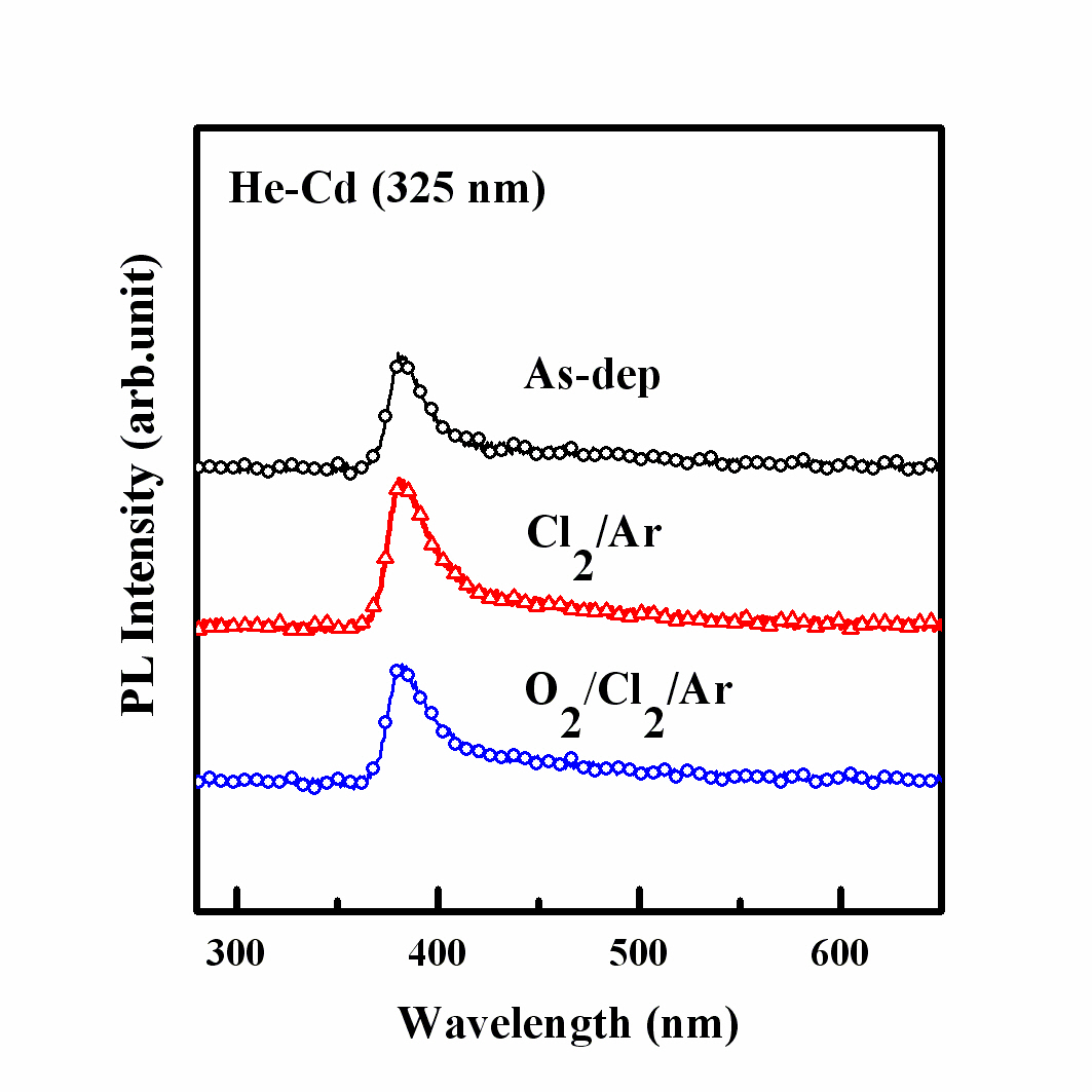
Figure 1 represents the etch rate of ZnO as a function of the Ar gas content in the Cl2 plasma. The maximum etch rate of the ZnO thin film in the Cl2/Ar plasma was 40.3 nm/min at an RF power of 600 W, bias power of 200 W, and process pressure of 2 Pa. In our previous research and that performed by others, the chemical reactions on the ZnO thin film in the Cl2 plasma led to the formation of the compound, ZnxCly, from Cl radicals [5-8]. The
volatile byproduct was Zn-Cl compound which has a melting point of 290℃. Also, the ion bombardment of the Ar ions supported the chemical reaction of Cl2 by breaking the zinc-oxide bonds. However, the results of the etch rate experiments indicate that the presence of Ar gas above a certain amount causes the etch rate to decrease.
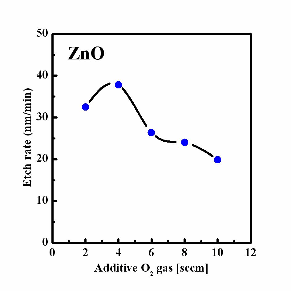
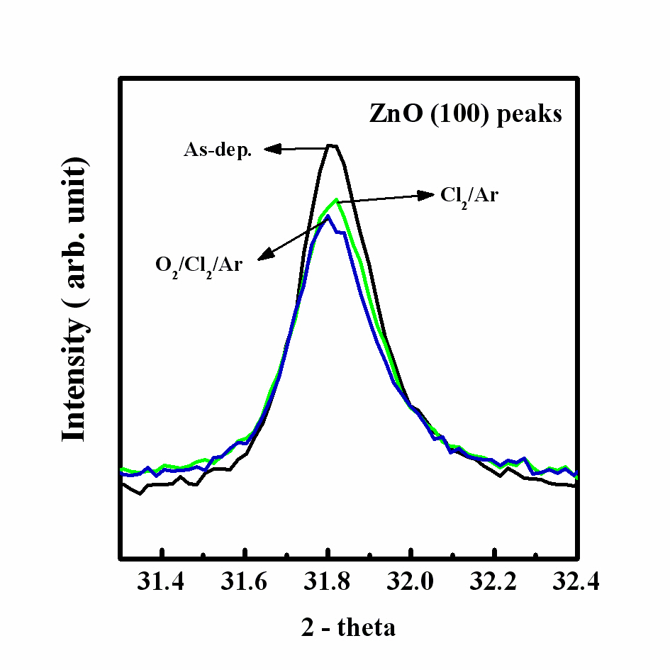
We performed an O2 additive experiment under the previous Cl2/Ar experimental conditions, viz. a Cl2/Ar gas mixing ratio of 15:5 sccm, that showed the highest etch rate. The process pressure was 2 Pa, the RF power was 600 W, and the bias power was 200 W. Figure 2 shows the etch rate of ZnO over quartz as a function of the O2 content in the Cl2/Ar plasma. The etch rate of the ZnO thin film at an O2 flow rate of 4 sccm was 37.8 nm/min. As the O2 content increased up to 10 sccm, the etch rate of the ZnO thin film was increased to 19.9 nm/min. As the O2 content was increased in the Cl2/Ar plasma, the etch rate of the ZnO thin films decreased. Figure 3 shows the XRD 2θ patterns of the ZnO film etched using a Cl2/Ar sccm gas mixing ratio of 15:5 and an O2/Cl2/Ar gas mixing ratio of 4:15:5 sccm and of the as-deposited
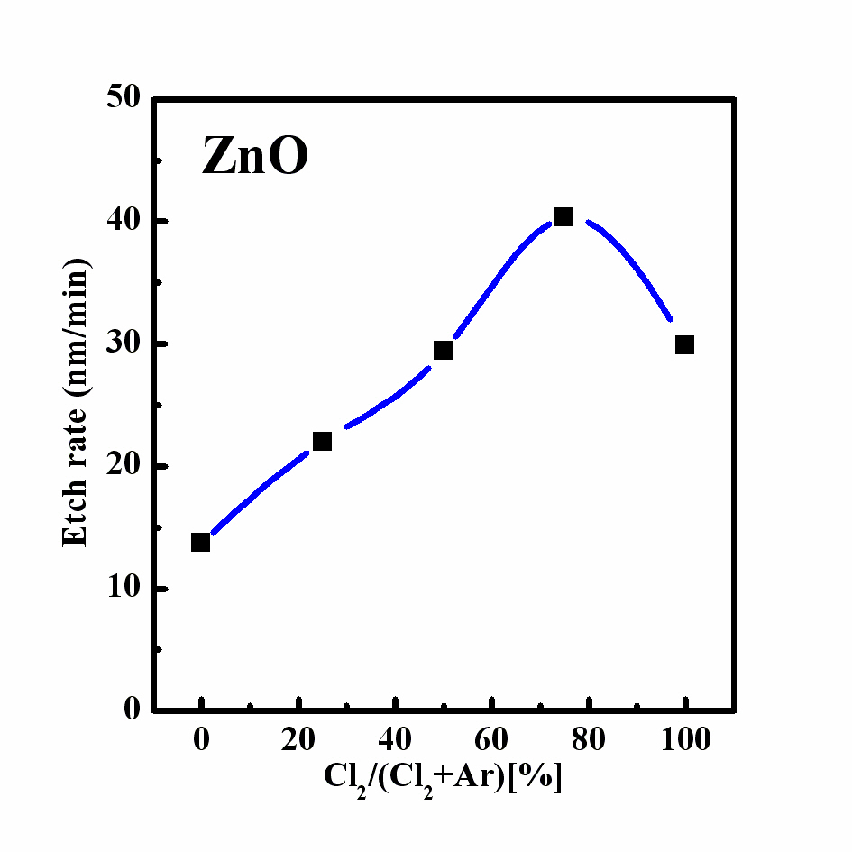
sample. The experimental conditions included an RF power of 600 W, bias power of 200 W and process pressure of 2 Pa, The XRD pattern of the ZnO thin films was used to investigate the change in the crystal structure during plasma etching with Cl2 based chemistry. As shown in Fig. 3, a strongly oriented (100) peak and weak (002) and (110) peaks were detected in the XRD patterns of all of the samples [9-11]. We assume that the ALD method leads to the formation of a mainly one directional crystal structure. The XRD pattern of the films etched in the Cl2/Ar plasma was similar to that of the as-deposited sample. However, the fluctuation of the intensity of each peak means that the metal chloride compounds, ZnxCly, volatilized during the etching of the ZnO thin films. In this work, we assume that the chemical reaction of the Cl radicals and ion bombardment of argon gas are responsible for the changes in the properties of the ZnO thin film, including its crystallinity, and that the deposition method employed (ALD) inhibits the creation of a poly or amorphous structure.
Figure 4 shows the intensity of the (100) peaks in each gas
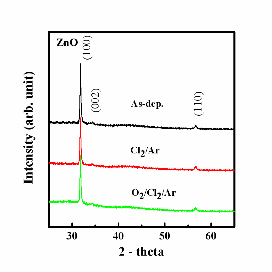
[Table 1.] Variation of FWHM and grain size of the XRD (002) peaks with the plasma

Variation of FWHM and grain size of the XRD (002) peaks with the plasma
mixture at a fixed RF power of 600 W, bias power of 200 W, and process pressure of 2 Pa. The results of the XRD analysis showed that the peak intensities of the etched ZnO thin films differed from those of the as-deposited sample. The (100) peak of the as-deposited film shows the high intensity, while those of the samples decreased with the increased O2 content. The (100) peak intensity was decreased after etching in the Cl2/Ar plasma.Also, the intensity of the (100) peak of the film etched in the O2/Cl2/Ar plasma was lower than that of the as-deposited sample.Moreover, the XRD peak of the film etched in the Cl2/Ar plasma was shifted to a higher diffraction angle. This indicates that the
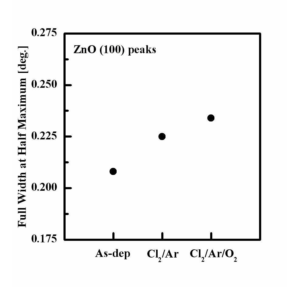
etched sample in the Cl2/Ar plasma experience more stress,whereas the etched sample in the O2/Cl2/Ar plasma shows less stress [12,13]. These observations allow us to assume that the use of the Cl2-based chemistry during the etching process highly modifies the ZnO thin film crystal structure. We suggest that the Ar ion bombardment induces stress in the ZnO thin films and decreases the intensities of the XRD peaks caused by the chemical reaction with Cl and O radicals, which changes the chemical purity of the ZnO thin film. Figure 5 shows the full width at half maximum (FWHM) value of the (100) peak of the film etched in the Cl2/Ar gas mixture and the FHWM values and grain size calculated using Scherrer’s equation for each plasma chemistry are shown in Table 1. The XRD diffraction results indicate that the ion bombardment and chemical reaction change the crystalline structure of the ZnO thin film. In the Cl2/Ar plasma chemistry, the FWHM value was increased and the grain size was decreased, indicating that the crystallinity of the ZnO thin films was modified by the ion bombardment or chemical reaction. Also, the O2/Cl2/Ar sample has a higher FWHM value and lower grain size than the other films. In previous experiments, the shift of the FWHM value to a high value indicated that the crystalline structure was changed [9-11] and this change in the grain size influenced the physical properties of the thin films. According to the FHWM values and grain size, the modification of the physical properties of the ZnO thin films can be explained by the chemical reaction of the Cl radicals, which make it difficult for the films to keep their original crystalline structure. Also, the FWHM value of the O2/Cl2/Ar sample is very different from that of the as-deposited one, indicating that the O2 gas affects the crystal structure and crystallinity. As a result, it can be concluded that the small perturbations of the FWHM value (~0.1 θ) correspond to the damage or modification of the crystallinity induced by the plasma etching, which was mainly caused by chemical reactions.
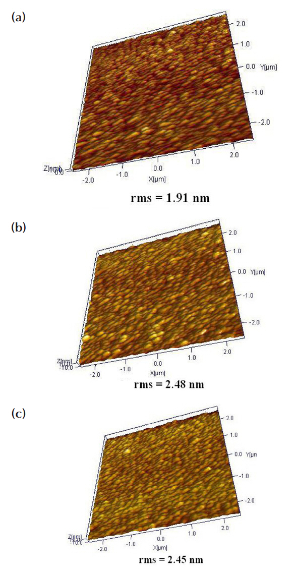
Figure 6 shows the three-dimensional (3D) AFM images of the ZnO thin films etched in the Cl2/Ar = 15:5 sccm plasma and O2/Cl2/Ar = 4:15:5 sccm plasmas. The experimental conditions were a fixed RF power of 600 W, bias power of 200 W, and process pressure of 2 Pa. Figure 6(a) show that the rms roughness of the asdeposited sample was 1.91 nm. As shown in Figs. 6 (b) and (c), the ZnO thin film samples which were etched using the Cl2/Ar =15:5 sccm and O2 /Cl2 /Ar = 4:15:5 sccm plasmas had rms roughnesses of 2.48 nm and 2.45 nm, respectively. Thus, the etched samples generally had higher rms roughnesses than the as-deposited one. However, the O2/Cl2/Ar plasma sample had a lower rms roughness than the Cl2/Ar plasma sample.
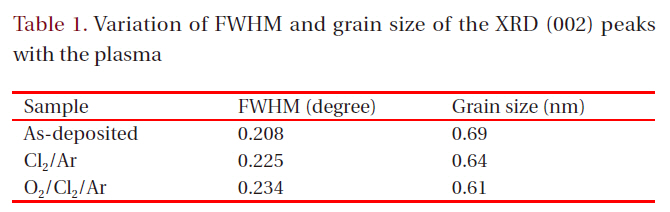
We obtained the photoluminescence spectra of the ZnO thin films at room temperature. Figure 7 shows the PL spectra of the ZnO thin films in the as-deposited state and after etching using the Cl2/Ar = 15:5 sccm and O2/Cl2/Ar = 4:15:5 sccm plasma chemistries.The experimental conditions were a fixed RF power of 600 W, bias power of 200 W, and process pressure of 2 Pa. The films etched in the Cl2/Ar and O2/Cl2/Ar plasma chemistries showed similar PL spectra to those of the as-deposited sample. The PL spectra of the as-deposited ZnO thin films showed a strong band-edge luminescence at 380 nm (3.26 eV) and absence of any deep-level emission (2.4~2.6 eV), while those of the samples etched in both the Cl2/Ar and O2/Cl2/Ar chemistries also showed the same band-edge luminescence with increased intensities and no deep-level emission. In etching experiment, the bandedge luminescence of the ZnO thin film, which was deposited on a quartz substrate using the atomic layer deposition method, was improved such that it has a strong band-edge luminescence and no deep-level emission. According to previous studies, the plasma induced damage and native defects, such as O vacancies and Zn interstitials, contribute to the creation of a deeplevel emission [4,14,15]. However, no deep level emission was found in the PL spectra of the ZnO thin films prepared in this work, which means that there were no native defects in the ZnO samples, as compared to those of the ZnO thin films deposited by sputtering which showed strong deep level emissions [15,16]. The etched ZnO sample prepared using ALD showed better band-edge luminescence and no deep level emission, indicating that this method produces films having better quality than those prepared by the sputtering method.
We investigated the plasma induced damage and modification of ZnO thin films etched using a Cl2/Ar plasma alone and one to which O2 gas was added for the dry etching process. The plasma gas chemistry influenced the physical and optical properties of the ZnO thin film. When the experimental condition was an RF power of 600 W, bias power of 200 W, gas mixture of Cl2/Ar = 15:5 sccm, and process pressure of 2 Pa, the maximum etch rate of 40.3 nm/min was obtained for the ZnO thin films. Also, the etch rate of the ZnO thin film at an O2 flow of 4 sccm was 37.8 nm/min. As the O2 content increased up to 10 sccm, the etch rate of the ZnO thin film was decreased. In the XRD analysis, a strongly oriented (100) ZnO peak and weak (002) and (110) ZnO peaks were detected. The high FWHM values obtained in the XRD analysis of the ZnO thin films indicates that the plasma chemistry modifies or damages their physical properties. According to the 3D AFM image, the surface roughness of the as-deposited sample was 1.91 nm. However, the surface roughnesses of the etched samples, viz. 2.48 nm in the Cl2/Ar plasma and 2.45 nm in the O2/Cl2/Ar plasma, were the higher than that of the asdeposited sample. In the conventional dry etching mechanism,the ion flux and ion bombardment of inert gas ion promote the physical etching mechanism and chemical reactions by breaking the bonds of the chemical compounds. From the XRD and AFM analysis, it was found that the film etched using the O2/Cl2/Ar plasma chemistry showed a low rms roughness, high FWHM value and large grain size. The oxygen ions cause the low rms roughness and have an influence on the chemical reactions during etching, leading to the large FWHM value and grain size. Therefore, we suggest that the plasma gas chemistry during the etching process contributed to the modification of the crystal structure and grain size, however the resultant plasma induced damage was insufficient to reduce the optical properties. For this reason, further studies using chemical analysis are required to clearly explain the relation between the PL intensity and plasma chemistry in the case of ZnO thin films.