Non-volatile semiconductor memory devices are mainly based on floating gate devices and quantum trap devices. The increasing demand for low power, low voltage, high reliability, high program/erase speed and low manufacturing costs for high density EEPROMs (electrically erasable programmable read-only memories) has been the driving force for quantum trap devices, especially SONOS (polysilicon-oxide-nitride-oxide-silicon) devices, the most attractive candidate [1,2].
We developed an embedded SONOS process using 0.25 ㎛ technology that allows for the implementation of non-volatile SONOS memory cells along with high performance 2.5 V logic transistors and 3.3 V I/O’s on the same chip with only four additional mask steps.
However, our system severely suffered from ONO rupture failures that occurred during endurance cycling. A significant percentage of customer sample parts experienced catastrophic NV (Non-Volatile) failures prior to reaching the endurance test goal and we have made every effort to resolve this endurance failure [3,4].
1.1 The phenomena of ONO rupture
More than 10% of the parts failed before reaching 1,000 cycles. However, a very high percentage of parts that passed 1,000 cycles did not fail for up to 1,000,000 cycles and beyond [5,6]. The source of this endurance failure was not caused by a shift in the threshold voltage but by an ONO rupture in some failed bits, which originated from weak spots such as pin holes, particles, chemical contamination, surface roughness, local thinning, substrate defects, causing the 2 Mb SONOS gate array current to increase from about 6 μA to 1 mA.
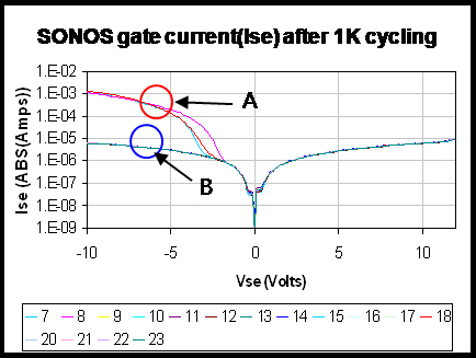
This caused an additional load on the negative charge pump,which in turn caused a full array NV (Non-Volatile) failure due to a weakened store cycle, as seen in Fig. 1.
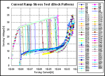
Figure 2 shows the positive current ramping stress test results used to characterize the ONO rupture failure. This exhibited that our current embedded SONOS process possessed a very severe reliability issue caused by a lack of ONO quality.
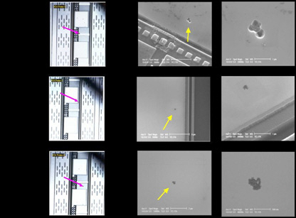
Figure 3 shows the ONO rupture failure points in the planar type ONO capacitor test pattern that were found by the optical beam induced resistance change (OBIRCH) test and de-processing and therefore shows us that localized weak ONO spots are responsible for the ONO rupture failures. Therefore, we must quantify the ONO rupture failure in order to obtain a reliable embedded SONOS Process [7,8].
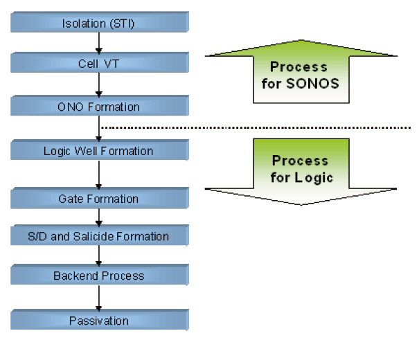
Figure 4 shows the simple flow of our current embedded SONOS process using 0.25 ㎛ technology. Basically, in order to preserve the characteristics of the logic transistors and other components already set up in our manufacturing line, all of the additional implemented steps for the SONOS transistor needed to be processed before the logic CMOS well formation process.
In this paper, we present only the SONOS transistor formation process with the exception of the logic CMOS formation process. The first active areas were defined by photolithography and etching processes. The first active areas are areas in which the SONOS transistor, logic transistors, and other components were formed. After the formation of the active areas, additional implantation, called the Cell Vt implant, was performed in order to adjust the threshold voltage of the SONOS transistor to about~0 V using phosphorus. Then the ONO multi-dielectric layer was deposited onto the whole wafer area, followed by a densification process. After the ONO multi-dielectric layer deposition and densification process, the ONO multi-dielectric layer regions, in which the SONOS transistor was formed, were defined through the photolithography and etching processes. After the ONO regions for the SONOS were defined, the logic well was formed and the p-well regions for SONOS transistor were formed through this logic well process. Thereafter, all of the remaining processes remained the same as the conventional logic CMOS process and therefore the detailed process sequences are not shown here.
We focused on the fact that in our embedded SONOS process, the Vt adjustment implantation, the punch-through implanta-
tion, the channel stop implantation as well as the pwell implantation for the logic NMOS transistor were directly introduced
into the ONO for the SONOS transistor, so we postulated that the ONO rupture failure of the SONOS was due to process induced ONO damage, not by bad intrinsic ONO quality, emphasizing ONO implantation damage. To demonstrate our hypothesis on the root-cause of the ONO rupture failure,
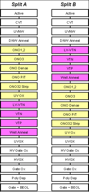
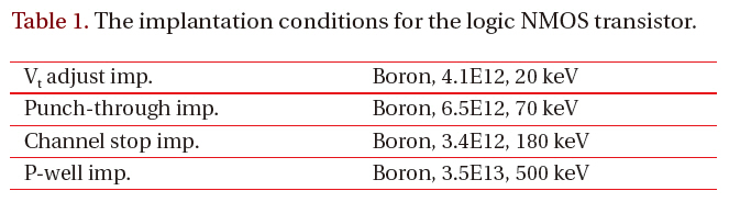
we prepared two kinds of samples. One was processed with our current embedded SONOS process (Fig. 5 Split A) and the other was processed with a new embedded SONOS process (Fig.5 Split B), in which we transferred all of the well implantation processes from the after ONO multi-dielectric layer deposition process to a before ONO multi-dielectric layer deposition process. Table 1 represents the detailed implantation conditions for the logic NMOS transistor.
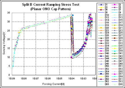
For the examination of ONO rupture reliability, a planar type ONO capacitor test pattern (area = 21,000 ㎛2) was submitted to an accelerated test using positive current ramping stress measurements. Figure 6 shows the positive current ramping stress test results in the new process group (Split B) in which all of the well implantation processes were fulfilled before the ONO multidielectric layer deposition process. It showed a very good and uniform ONO quality in comparison to the current embedded SONOS process.
[Table 1.] The implantation conditions for the logic NMOS transistor.

The implantation conditions for the logic NMOS transistor.
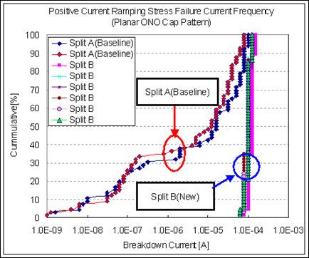
Figure 7 represents the failure current frequency in the positive current ramping stress test in the planar type ONO capacitor test pattern. The 1 μA positive stress current for 34 μs was thought to be a marginal current level for the ONO rupture failure screening,so therefore, the ONO rupture failure would be over 30% in our current embedded SONOS process (Split A), whereas it would never occur in the new embedded SONOS process (Split B). It was very evident that the ONO implantation significantly degraded the ONO quality and was completely responsible for the ONO rupture reliability issue in the current embedded SONOS process.
Thus, we can obtain an ONO rupture free embedded SONOS process with a very good and a very reliable ONO quality by switching all of the well implantation processes from after the ONO multi-dielectric layer deposition process to before the ONO multi-dielectric layer deposition process.
3.2 Implantation damage mechanism
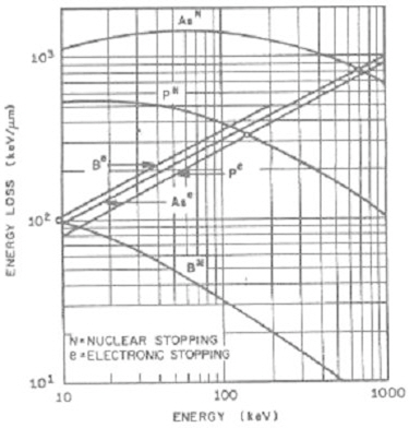
As an implanted ion moves through a solid target such as silicon, silicon dioxide, or silicon nitride, it transfers energy by colliding with the target nuclei, which is referred to as nuclear collisions, and by coulombic interaction with the electrons in the target material, which is referred to as electronic collisions.In the latter mechanism, the energy transferred to the electrons can lead to the excitation of the electrons to higher energy levels, or to ionization by the ejection of electrons from their atomic orbits. The energy loss due to such target interactions gradually slows the implanted ion, eventually bringing it to a stop. The total rate of energy loss of an implanted ion is given by the sum of the energy loss through nuclear collisions and electronic collisions. Fig. 8 shows that the nuclear stoppage increases at low energies, reaches a maximum at some intermediate energy, and decreases at higher energies, because at a high velocity the implanted ions move past the target nuclei too quickly to efficiently transfer energy to them. It is important to note that the energy loss due to nuclear collisions increases with the mass of the implanted ion and thus heavy ions, such as arsenic or phosphorus, will transfer much more of their energy through the nuclear collisions than light ions, such as boron. When energetic ions strike a solid target, they lose their energy in a series of nuclear and electronic collisions. However, only the nuclear collisions result in the displacement of the atoms which compose a solid target. If the energy transferred to the atom of a solid target is less than the required energy needed to displace it from its lattice site, no displacement event occurs but if the energy transferred to the atom of a solid target is more than the required energy needed to displace it from its lattice site, a single point defect, multiple defects, or defect clusters are created.
As shown in Fig. 8, at the initial impact energies, most of the energy loss for the light ions, such as boron, is due to electronic collisions which do not produce displacement damage. However, as the boron ions penetrate deeper into the lattice of a solid target, they lose energy and eventually, a cross-over point is reached, below which nuclear stopping predominates. Thus, most of the solid target lattice damage occurs in the part of the light ion trajectory that is beyond that point.
As shown in Table 1, the implantations through the ONO multi-dielectric layer consist of four steps, which are the Vt adjust implantation, the punch-through implantation, the channel stop implantation and the pwell implantation and according to Fig. 8, in the case of over an 180 keV boron ion has an initial nuclear energy loss of less than 2 eV/ A. Thus, the boron ion will lose less than 5 eV from nuclear collisions for each lattice plane of silicon, silicon dioxide and silicon nitride. Since 5 eV is less than the displacement energy in the silicon, silicon dioxide and silicon nitride lattices at the initial implantation stage, it does not displace the atom of the lattice through nuclear collisions. Therefore the channel stop implantation and pwell implantation scarcely produced any displacement defects in the block oxide, trap nitride, tunnel oxide as well as the silicon surface because their implantation energies are all over 180 keV. However, in the case of a less than 70 keV boron ion, the initial nuclear energy loss was greater than 4 eV/A. Thus the boron ion will lose more than 10 eV from nuclear collisions for each lattice plane of silicon, silicon dioxide and silicon nitride. This 10 eV or more is able to displace the atom from the silicon, silicon dioxide and silicon nitride lattice site at the initial implantation stage. Therefore the punch-through implantation and the Vt adjust implantation can make displacement defects in the block oxide, trap nitride, tunnel oxide as well as the silicon surface because their implantation energies were all less than 70 keV. Although many of these displacement centers were recovered by the following thermal annealing, some damages never healed so these remaining displacement centers increased the leakage current and the rupture failure of the ONO multi-dielectric layer, and decreased the charge-to-breakdown and the breakdown voltage of the ONO multi-dielectric layer.
We appended the ONO deposition process to the beginning of the 0.25 ㎛ embedded SONOS process before all of the logic well implantation processes in order to maintain the characteristics of the basic CMOS logic technology. This caused severe ONO rupture failure. We postulated that the ONO rupture failure originated from the ONO implantation damages and prepared two kinds of samples to investigate this issue: one sample was processed with the current embedded SONOS process and one sample was processed with a new embedded SONOS process in which all of the logic well implantations were performed before the ONO deposition process. Through these investigations, we demonstrated that the ONO implantation damage was the root cause of the ONO rupture failure in the current embedded SONOS process.
According to the implanted ion’s energy loss model, both the Vt adjustment implantation and the punch-through implantation mainly caused the displacement damages in the block oxide, trap nitride, tunnel oxide as well as in the silicon surface through nuclear collisions in the current embedded SONOS process.
Consequently, we can obtain an ONO rupture free embedded SONOS process with a very good and reliable ONO quality if we only transfer all of the logic well implantation processes from after the ONO deposition process before the ONO deposition process.