Field emission displays (FEDs) have recently gained a great amount of attention since FEDs are considered next-generation technology for flat panel displays that will replace the cathoderay tube (CRT). Sulfide-based phosphors have been used in the CRT. However, if sulfide-based phosphors are used as low-voltage phosphors in the FED, an inherent problem will be encountered of which the lifetime in the FED will be limited since the sulfidebased phosphors contaminate the field emission cathode. However,oxide phosphors offer potential advantages because of their superior stability under electron bombardment and excellent luminescence properties [1].
Researchers have allotted attention to oxide phosphors and how they operate at low voltages. The application of low-voltage phosphors in FEDs must comply with the following requirements. Since an electric charge of a cathode can be accumulated on the phosphor surface by incident electrons, the first criterion requires the phosphor to be conductive. The emission-starting voltage must be low and the efficiency should be high. Second, the processes comprising the emission and excitation of the phosphor should not generate hazardous materials. The amount of discharge of hazardous substances in the heating process during FED manufacture should be low. Third, a stable phosphor surface, long life, short afterglow time, small particle size, and excellent phase splitting characterization are necessary [2].
Zinc gallate is a potential candidate among oxide phosphors for low-voltage cathode luminescence devices. The structural formula of zinc gallate is AB2O4; additionally, zinc gallate encompasses a cubic structure that consists of rock salt and zinc blende structures as well as a normal spinel structure [space group of Fd3m(Oh 7)][3]. The ZnGa2O4 host lattice is a normal spinel crystal structure with Fd3m space group, and it has tetrahedrally coordinated Zn sites (Td) surrounded by 4 oxygen ions and octahedrally coordinated Ga sites (Oh) surrounded by 6 oxygen ions. ZnGa2O4 is a normal spinel crystal structure with Fd3m space group [4]. The 32 oxygen ions are C3V sites arranged in a close-packed cubic formation leaving 64 tetrahedral (Td) and 32 distorted (D3d) sites. Also, ZnGa2O4 is an ultraviolet-transparent conducting oxide with a wide energy band gap of about 4.4 eV and a moderate conductivity can be achieved by annealing under a reducing atmosphere at high temperature [5].
In order to manufacture thick films out of these phosphors, a suitable manufacturing method, such as screen printing, sol-gel,jet printing and tape casting, must be employed according to the field of application. Recently, screen printing has actively progressed because of its ability to mass produce uniform and highresolution thick films at low-costs [6].
Trivalent chromium (Cr3+) is the most stable oxidation state of chromium; thus, it is widely used as a luminescent dopant and luminescence sensitizer in various materials. Chromium is a low cost activator, which provides deep color and bright luminescence. For instance, the color of many natural and synthetic gemstones, such as rubies, emeralds, and alexandrite, is caused by Cr3+ ions. Consequently, Cr3+ has been subject to numerous optical spectroscopic and luminescence investigations. Furthermore, Cr3+ doped systems have been applied to modern technologies including tunable solid-state lasers, high temperature sensors and high-pressure calibrants [7].
In this study, Mn2+ ions, a green luminescence activator, and Cr3+ ions, a red luminescence activator were separately doped into ZnGa2O4 through the precipitation method. The ZnGa2O4 was then screen printed onto an indium tin oxide (ITO, 2.8T) substrate. Various film thicknesses were applied to the manufactured substrate. The formation of the spinel phase and the luminescence characteristics of ZnGa2O4 were observed at various thicknesses.
2.1 Preparation of ZnGa2O4 phosphor
ZnGa2O4 phosphor powder was prepared through the precipitation method. ZnSO4 · 7H2O (99.99%; Sigma Aldrich) and Ga2(SO4)3 · xH2O (99.99%; Sigma Aldrich) were used as starting materials and aqueous NH4OH (NH3 content 28-30%; Sigma Aldrich) was used as the precipitant. The starting solutions were prepared by dissolving equimolar amounts of zinc sulfate and gallium sulfate in distilled water (final concentration 0.1 mol/dm3) to achieve a metal-atom ratio of Zn/Ga = 1/2. A 0.89 mol/dm3 aqueous ammonia solution was prepared and used in the experiments. The starting metal solution was added to the aqueous ammonia solution at 90℃ upon stirring (this was done at a rate of 1.5 ml/min and over 20 hours). The metal ions were rapidly hydrolyzed by ammonia, and precipitation occurred spontaneously. The precipitation experiment was performed using a reflux system to preserve the concentrations over the experimental period. The precipitates were separated by filtration through a membrane filter, washed with distilled water, and then dried for 4 hours in an oven at 60℃. The nanocrystalline ZnGa2O4 powders thus obtained, were sieved to deagglomerate the particles and then sintered in furnace for 1 hour at temperatures of 1,000℃.
ZnGa2O4: Mn2+ powder was prepared by adding 0.006 mol/dm3 MnSO4 · xH2O (99.99%; Sigma Aldrich) to zinc sulfate and gallium sulfate mixed powder. ZnGa2O4: Cr3+ powder was prepared by adding 0.002 mol/dm3 Cr2(SO4)3 · xH2O (99.999%; Sigma Aldrich)to zinc sulfate and gallium sulfate mixed powder.
2.2 Preparation of thick films
The phosphor thick films were prepared through the screen printing method. The ZnGa2O4 phosphor powder was dispersed in binder (PET transparent ink) with a weight ratio of 6:4, and the phosphor thick film was deposited on the ITO glass (2.8T) by screen printing using an automatic screen printer from Microtec Co. (Japan). The manufactured thick films were dried for 2 hours in an oven at 80℃.
The morphology and thickness of the manufactured thick films were observed by field emission-scanning electron microscopy (FE-SEM; Hitachi S-4700, Japan). Cathodeluminescence (CL) was measured using an environmental SEM with a Mono-CL application, FEI Corporation (Hillsboro, OR USA).
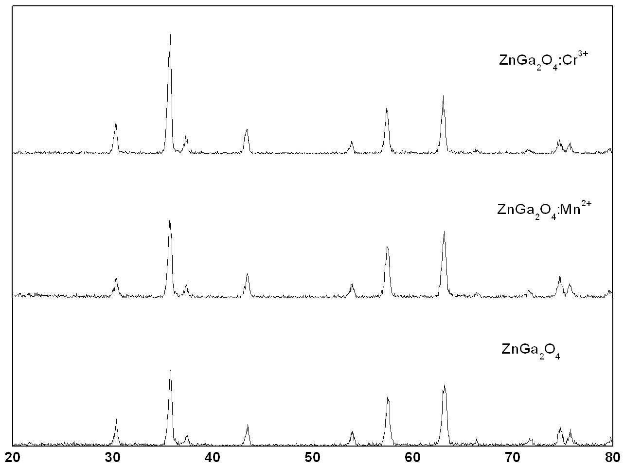
X-ray diffraction (XRD) patterns of ZnGa2O4, ZnGa2O4:Mn2+, Cr3+ phosphors are shown in Fig. 1. XRD patterns agree well with JCPDS 38-1240, indicating that the obtained samples are single phase. The ZnGa2O4 host lattice is a normal spinel crystal struc-
ture with Fd3m space group, and it has tetrahedrally coordinated Zn sites (Td) surrounded by 4 oxygen ions and octahedrally coordinated Ga sites (Oh) surrounded by 6 oxygen ions [4]. ZnGa2O4 phosphors have a cubic normal spinel crystal structure. Two dopants of Mn2+ and Cr3+ in ZnGa2O4 phosphors are expected to be substituted for tetrahedral sites of Zn2+ and octahedral sites of Ga3+ respectively to minimize charge and size difference [4].
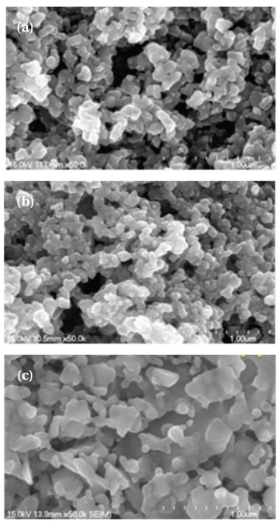
Figure 2 shows SEM images of ZnGa2O4, ZnGa2O4:Mn2+, Cr3+ phosphors. The actual particle size of nanosized ZnGa2O4, ZnGa2O4:Mn2+, Cr3+ is a regular spherical shape between 50 nm and 100 nm.
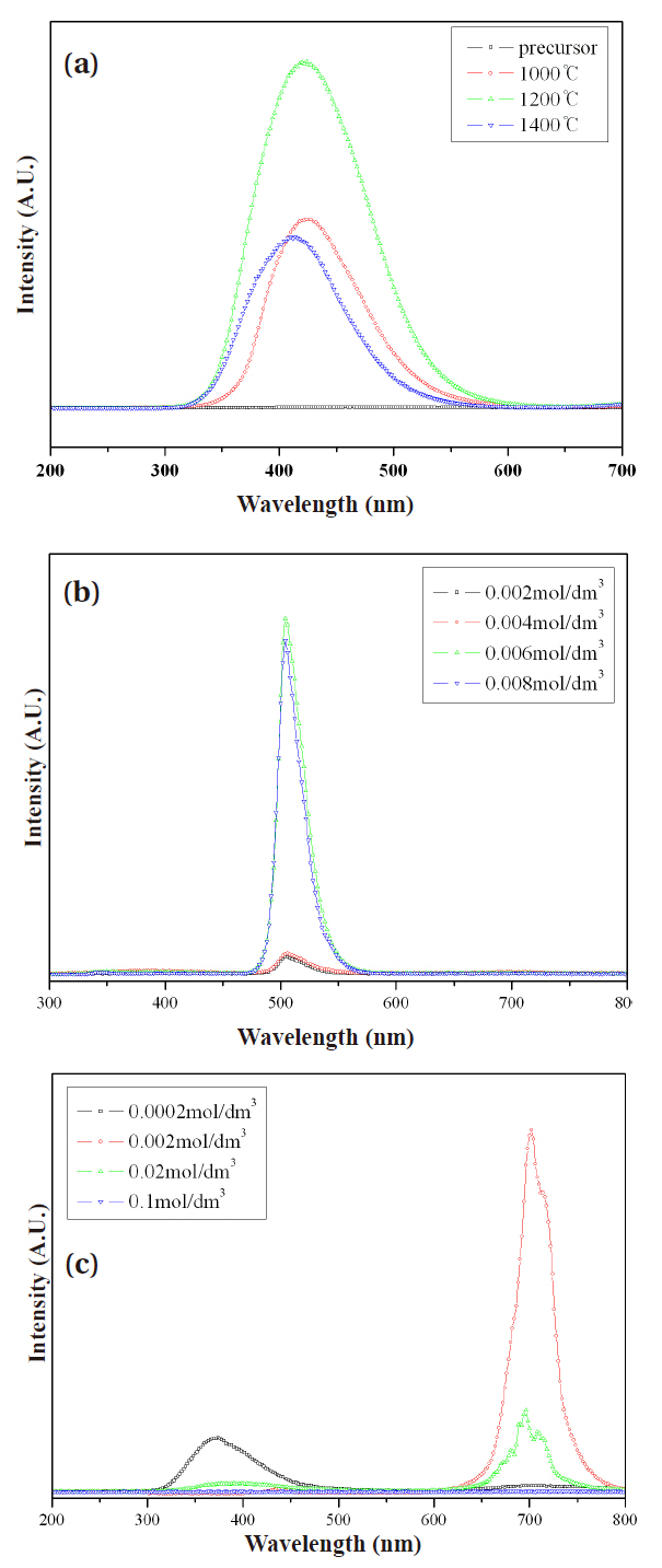
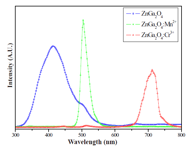
The CL spectra of ZnGa2O4, ZnGa2O4:Mn2+, Cr3+ phosphors are depicted in Fig. 3. All CL spectra are normalized to the green
emission intensity. The 420 nm CL peak originated from the charge transfer of Ga-O [8]. The 505 nm CL peak originated from 4T-6A 3d intrashell transition of Mn2+ [9]. The 705 nm CL peak originated from 2E-4A2 3d intrashell transition of Cr3+ [10].
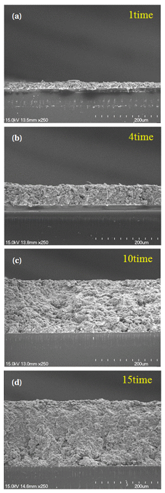
Figure 4 shows sectional images of the ZnGa2O4 phosphor
films at various thicknesses. The thickness of the films proved to be arithmetically inaccurate. This inaccuracy was attributed to the deposition of particles from the upper layer onto empty spaces of the bottom floor, which occurred during the binder’s drying process after screen printing.
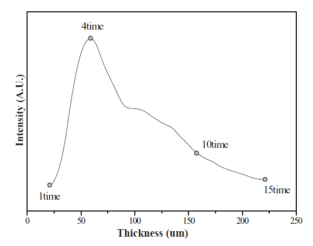
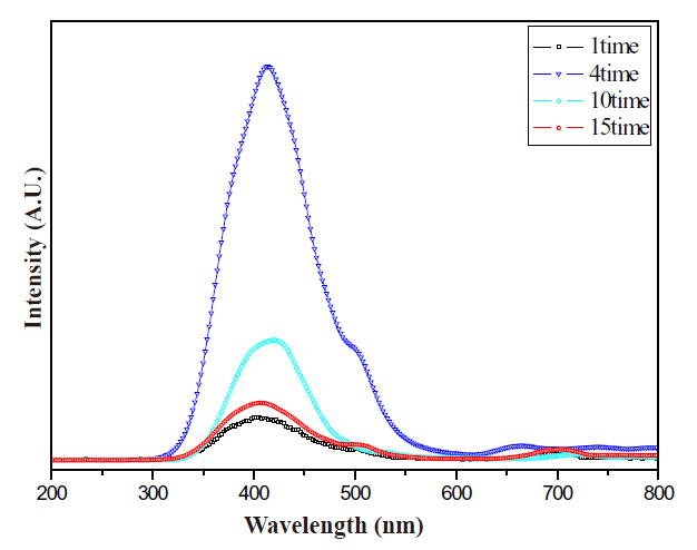
Comparisons regarding the CL spectra and luminescence intensities of the ZnGa2O4 phosphor thick films at various thicknesses are displayed in Figs. 5 and 6. The characteristics of the phosphor thick films were improved by increasing the thickness of the phosphor thick films, and its intensity reached a maximum at a thickness of the 60 ㎛. When the thickness increased over 60 ㎛, the luminescence intensity decreased by a certain amount of degrees. result was attributing to the following explanation: when the accelerating voltage was inflicted, the luminescence efficiency of the incidence energy was maximized at a phosphor film thickness of 60 ㎛; however, when the thickness of the thick films ran over 60 ㎛, after the incidence energy was distributed into the inner part of the thick films, the luminescence efficiency and intensity decreased because diffusion of the photon and absorption of the phosphor increased.
Figure 7 shows CL spectra of the ZnGa2O4, 0.006-mol/dm3-Mn2+-doped ZnGa2O4: Mn2+ and 0.002-mol/dm3-Cr3+-doped ZnGa2O4: Cr3+ phosphor thick films. The emission spectrum of ZnGa2O4 exhibited a blue emission band and activation with Mn2+ or Cr3+ ions that shifted the emission to green or red, respectively.
In this study, ZnGa2O4: Mn2+, Cr3+ phosphors were synthesized through the precipitation method. The effects of the activator Mn2+, Cr3+ concentration on the changes the luminescent properties were investigated. The ZnGa2O4: Mn2+, Cr3+ phosphors exhibited three colors; a blue band of 430 nm from the charge transfer between Ga-O, a green band of 505 nm from Mn2+ and a red band of 705 nm from Cr3+. The ZnGa2O4, ZnGa2O4:Mn2+,Cr3+ phosphors actual particle size of nanosized ZnGa2O4, ZnGa2O4:Mn2+, Cr3+ was a regular spherical shape between 50 nm and 100 nm.
The thick films of the ZnGa2O4 were deposited with the various thicknesses using the nano-sized powder. The best luminescence characteristics were shown at a thickness of 60㎛. When the thickness of the films increased over 60 ㎛, the luminescence intensity decreased by a certain amount of degrees. Additionally, the blue-emission ZnGa2O4, green-emission ZnGa2O4:Mn2+ and red-emission ZnGa2O4:Cr3+ phosphor thick films, which have superior characteristics, were manufactured by the screen-printing method. All CL spectra were normalized to the green emission intensity. The 420 nm CL peak originated from charge transfer of Ga-O [8]. The 505 nm CL peak originated from 4T-6A 3d intrashell transition of Mn2+ [9]. The 705 nm CL peak originated from 2E-4A2 3d intrashell transition of Cr3+ [10].
These results indicate that ZnGa2O4 phosphors prepared through the precipitation method and the thick films manufactured through the screen printing method have wide application like a movie as phosphor of the full color emission.