Transparent conducting oxides, such as zinc oxide, cadmium oxide, indium tin oxide, and indium zinc oxide, have recently received a large amount of attention because of their transparent, conductive properties and various applications. Among these transparent conducting oxides, zinc oxide (ZnO) is considered a promising II-VI compound for semiconductors, exhibiting a wide band gap of 3.35 eV and a wurtzite structure; it is a multifunctional material that can be applied to transparent electrodes,gas sensors, photovoltaic devices, blue and UV light emitters,and bulk acoustic wave devices [1].
Hydrogenated amorphous silicon thin-film transistors (a-Si TFTs) are widely used for consumer electronics and have been demonstrated to be useful for solar cells and flexible displays and other devices. However, applications of a-Si TFTs are limited by their low mobility and light sensitivity due to the material's intrinsic properties. Organic thin-film transistors and low temperature polysilicon have been examined for more advanced device applications. Recently, oxide thin film transistors, including amorphous oxide semiconductors have drawn much attention because of their high mobility, uniformity, processability and transparency.
ZnO TFTs were prepared by using different techniques. Prior studies investigating inorganic dielectric materials utilized sputtering techniques as a means to prepare active channel material [2-4]. Lee et al. [5] fabricated a top-ZnO TFT with a polymeric dielectric using radio-frequency sputtering at 100℃. Other researchers used an atomic layer deposition (ALD) technique for ZnO preparation [6]. Inorganic dielectric materials, such as aluminium oxide, have been regularly used for the oxide TFT devices. The use of organic dielectrics for TFTs is an ideal solution for the development of flexible electronics. One report exists elaborating on an oxide semiconductor with a polymeric gate dielectric fabricated by using ALD [7]. However, the investigation of an optimized structure of ZnO TFT with a polymeric dielectric is still greatly necessary.
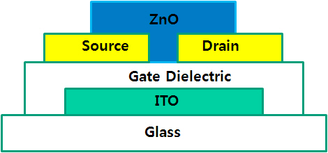
In this work, a bottom-gate and bottom-contact ZnO TFT with a poly-4-vinylphenol (PVP) dielectric material was prepared and optimized. The effect of thickness and width-to-length ratio of the ZnO active layer in a thin-film transistor was characterized.
Figure 1 shows a schematic view of the bottom-gate and bottom-contact ZnO TFT that was used in this study. Indium tin oxide (ITO) employed as the gate metal was patterned on a 100 × 100 mm2 glass panel using photolithography. PVP was spin coated with a crosslinking agent, poly (melamin-co-formaldehyde), in propylene glycolmonomethyl ether acetate on the ITO-patterned glass substrate and cured in a vacuum oven in
order to achieve a 450 nm thickness. The dielectric pattern was dry-etched using O2/NF2 for the contact open. Gold, which was used as a source and a drain, was deposited onto the substrate using a thermal evaporator and was patterned by using a liftoff process. The thicknesses of the source and the drain were 40 nm. The ZnO thin film that was used as a channel material was deposited on the cleaned substrate through ALD at a temperature of 150℃. Diethylzinc was used as a source for Zn. Oxygen plasma was used as an oxygen source for ZnO fabrication. The reactor pressure was maintained at 0.7 Torr with argon gas purging at 100 sccm. During the reaction, diethylzinc and the oxygen plasma were sequentially injected into the reactor chamber to form a ZnO monolayer on the substrate. The thicknesses of the active layer were 10, 20, and 30 nm, and the active layer was patterned by using photolithography. The TFT channel was varied in a width rang of 10-㎛ to 500-㎛ and with a length of 10-㎛. The thermal treatment of ZnO TFT was carried out in a hot plate chamber under an oxygen atmosphere at 200℃ for 1 hour. All current-voltage (I-V) characterizations of the ZnO TFT were carried out with a semiconductor parameter analyzer (Keithley 4200; Kiethley, Cleveland, OH, USA) in the dark at room temperature.
The bottom-contact structure for this study is shown in Fig.1. In order to produce an oxide TFT possessing bottom-contact and a bottom-gate, ITO and gold (Au) were used as electrode materials. The ITO and Au were patterned through lithography and lift-off processes, respectively. These methods facilitated the acquirement of an adequate design rule. The ZnO thin film prepared through ALD was patterned by using photolithography in order to obtain a channel length of 10 ㎛. High quality ZnO thin films for transparent thin-film transistors were prepared by an injection type source delivery system related to ALD. By using this delivery system, the source delivery pulse time was reduced to 0.002 s, minimizing processing time and saving the precursor.The average growth rate was relatively normal, about 2.0 A°/cycle.
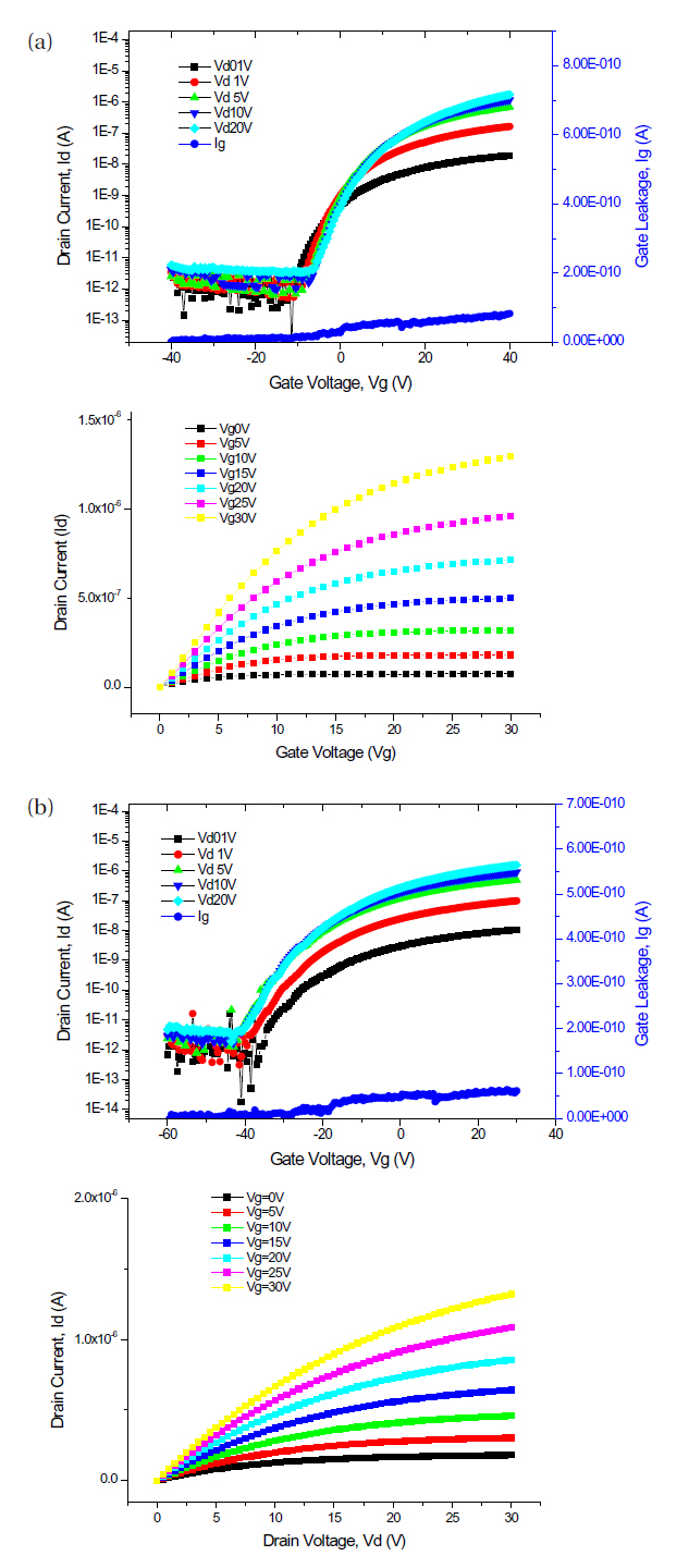
The transfer characteristics of various active layer thicknesses of ZnO TFTs are shown in Fig. 2. Figure 2 plots a set of log(Id) vs. Vg transfer curves of active layers measuring 20 nm and 30 nm in the ZnO TFT with different ranges of Vd from 10 mV to 20 V. The 10- and the 20-V curves are typical of such transfer characteristics, where Vd is sufficiently large so that the device operations are in a saturation state for this range of applied gate voltages. With different drain voltages, 100 mV to 20 V, the transition characteristics of the transfer curves show typical transfer regions from linear operation regions to saturation regions. The transition from linear operation to saturation occurs for a Vd between 1 V and 5 V because the 5-, 10-, and 20-V curves are almost overlaid upon one another. This Vd value is higher than the previously reported Vd of 100 mV. Hoffman [8] mentioned that
the observation of linear operation for a small Vd implied that drift was the dominant channel current mechanism rather than diffusion near the subthreshold region. As mentioned, for a polymeric gate insulator, the drift mechanism leads to a much higher voltage than it does for a silicon-oxide gate dielectric.
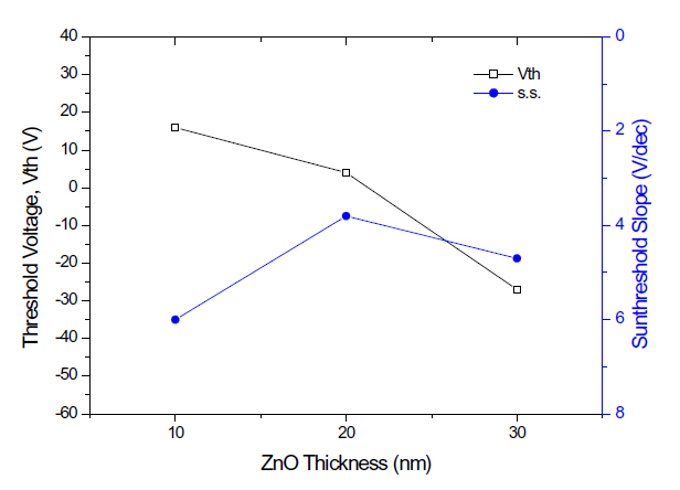
The threshold voltage (Vth) and the saturation mobility were obtained by fitting a straight line to the square root of the Id versus Vg curve from Fig. 2. The saturation mobility value was obtained at about 0.4 cm2/Vs. From this transfer characteristic,the range for the turn-on gate voltage (Vth) was approximately between -27 V to 17 V depending on the active thickness. Report-
edly, the threshold voltage shift to the negative region is due to an intrinsic property of the gate dielectric, the interface effect between the oxide semiconductor and the polymeric dielectric,and the free carrier density of ZnO [9]. However, our results suggest that the main cause for ZnO TFT by ALD is the active layer's film property regarding free carrier density. The various sources of free carrier density such as oxygen vacancies, zinc interstitials and hydrogen incorporations vary with the thickness of ZnO. The thicker active layer shows more sensitive behavior under atmospheric conditions. The thermal treatment around 200℃ can remove the absorbed hydroxyl group and improve the contact property; however, the treatment is not sufficient in order to minimize those defects in the structure.
From the transfer characteristics displayed in Fig. 2, we obtained a subthreshold gate swing that elucidates important information regarding performance parameters for display speed, low-power operation, and gray scale capability. The subthreshold swing, S, is defined as the gate voltage that is required to increase the drain current by a factor of 10. The subthreshold slope ranges from 4.0 to 6.0 V/dec. The slow transfer between the off and the on regions is due to the resistance between the gate-biasinduced conduction band and the source-drain electrons.
Figure 2 shows a set of drain current-voltage (Id-Vd) curves for discrete gate voltages (Vg) between 0 to 40 V for a fabricated ZnO TFT with a polymeric dielectric. These Id curves characteristic from linear to saturation behavior, like well operated general TFT systems. From the output characteristics, current crowding is not observed for active thicknesses of 20 nm and 30 nm, indicating acceptable contact resistance for the source-to-drain conduction. The output curves measured at Vd from 0 to 40 V exhibit clear pinch-off and solid saturation, indicating that the device follows the standard field-effect transistor theory and that the Fermi level in the channel is controlled by the gate voltage and the drain bias. However, the thinner layer of 10 nm exhibited poor contact at the linear region and saturation at lower gate voltages.
A different approach was reported on scaling behavior, varied channel width and length, of ZnO TFT prepared by sputtering technology with Al2O3/HfO2 dielectrics [10]. When the channel length was below 5 ㎛, the output characteristics exhibited deviation from hard saturation. TFT did not show saturation or output drain currents for channel lengths below 2 ㎛. Even though the report did not show the active layer thickness behavior of TFT, ALD-grown ZnO TFT with polymeric dielectric exhibited more robust behavior for the output characteristic by comparison. This behavior was not observed in organic TFT. For
pentacene TFT, mobility decreased with the thickness of the pentacene channel due to the parasitic resistance of the pentacene thickness, especially for the case of top contact for source/drain architectures [11].
According to Fig. 3, although the transfer curves exhibit acceptable TFT behavior, the thickness of active layer clearly affects the properties. Optimum thickness exists. A thickness of 20 nm shows more favorable transfer and output characteristics,as shown in Figs. 2 and 3. For active layer thicknesses ranging between 10 nm to 30 nm, ZnO TFT properties were influenced in a similar way. When the ZnO active layers were thicker, the threshold voltage showed a tendency to negatively shift while the subthreshold slope showed a little bit stiff slope. For thinner active layers, the threshold voltage shifted in the positive direction while the subthreshold slope showed a lower slope in comparison to other cases. The saturation behavior of the output curves also exhibited similar trends to Fig. 2. When the active layer of ZnO was 10 nm thick, the shift seen in the transfer characteristic at low Id with lower Vd is associated with the shortening of the channel length region and charge traps caused by weak zinc active layers with less drain voltage.
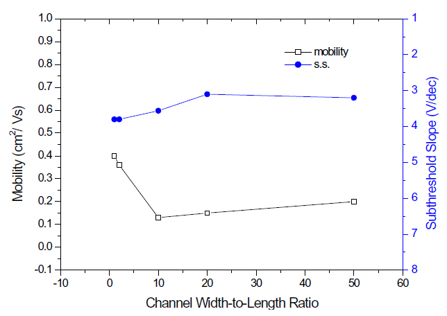
From Fig. 4, the width-to-length (W/L) effect for 20 nm ZnO TFT was examined. The mobility slightly decreased with the W/L ratio while the subthreshold slope became steeper. Similar results were reported by Fortunato et al. [4], suggesting that saturation mobility decreased as the W/L ratio increased due to the side wall effect associated with source/drain resistance as well as the fringing electronic-field effects that led to an additional current flow beyond the device edges. In poly-silicon TFT, the thin active channel layer exhibited a high current drive, but also showed poor source/drain contact and large parasitic series resistance.
In general, ZnO TFT operated in the enhancement mode because the drain current was zero at zero gate voltage and a positive gate bias was required for the onset of conduction. In this device, the ZnO TFT operated from the depletion mode to the enhancement mode because there were measurable drain currents at a gate voltage of 0 V for both cases, depending on the active layer thickness. As mentioned above, the main factor was the channel property rather than the gate dielectric. The gate dielectric also showed electrical instability due to the migration of ions and moisture-induced surface polarization under a negative bias [12]. The process may affect the interface which contains many positive traps that draw the electron charges for the channel current. ZnO TFT operation in the enhancement mode is favorable comparing depletion mode due to no gate voltage for switchoff, less power and simple design. ZnO TFT properties are greatly influenced by not only the device structure and the process conditions,but also the thickness of the active layer. The operating voltage and the threshold voltage are directly proportional to the active layer's thickness; thus, the structure of the device can be optimized in order to obtain desirable properties.
Different active layer thicknesses for ZnO bottom-contact TFTs were fabricated with a poly-4-vinyphenol polymeric dielectric through a process known as ALD. The threshold voltage of the ZnO TFTs shifted positively as the active layer thickness decreased and while the subthreshold slope decreased. The W/L ratio of ZnO TFT also affected the mobility and subthreshold slope due to the side wall effect and the fringing electronic-field effects. The ZnO TFT operated from the depletion mode to enhancement mode depending on the active layer thickness as a result of a ZnO film property regarding free carrier density. ALDgrown ZnO TFT with polymeric dielectric exhibited more robust behavior to the output characteristic. Such behavior was not observed in organic TFT. An optimized TFT structure possessed a mobility of 0.43 cm2/V s, a turn-on voltage of 0.85 V, a subthreshold slope of 3.3 V/dec, and an on-to-off current ratio of above 106 with solid saturation.