1. MAPPING OF HETROGENEOUS TECHNOLOGIES
To gain an economic advantage in the last decade many organizations have invested billions of dollars in research and development programs that span over a varied range of activities from smart pills for image sensing and monitoring, smart drug delivery for targeted therapy, through to more futuristic products based on memristive systems and metamaterials. The need for smart components has become evident and intelligent integrated circuits (I2C) based upon horizontal integration of radically differing technologies have been clearly identified as the driving force for future generation of products. As an example, a nanophotonic clinic based on system on chip (SoC) and system on system (SoS) technologies can be created using multifunctional nanoparticles in which therapeutic or monitoring agents are encapsulated and activated or monitored with either electromagnetic or light waves [1-3].
Embedded nano-based biophotonic sensors, for example that could be powered and monitored remotely to observe a wide range of physiological conditions such as status of internal tissues, blood sugar and oxygen level, blood pressure etc., would provide important enabling capabilities for robotic microsurgery.The integration of bio-devices with non-biological material provides higher performance in applications such as biomolecular motors for targeted drag delivery and bio-micro-electromechanical systems as analyte detector system with recognition capability of antigen-antibody. The ability to transmit and receive data efficiently will be a major challenge-as the consequence the‘first centimeter’ communication (body sensors and clothing) as part of the over-all communications strategy brings about new opportunities in health care and aged care environments.Such progress supported by bio-based technologies provide the foundation for a future in which information sensing, embedded processing, imaging and multi-level communication become pervasive [4,5].
Light-wave technology (photonics) synonymous with high speed networks is also beginning to show its footprint in areas that not so long ago appeared to be far removed from the conventional information communication technology arena. Photonics has always been viewed as an alternate to electronic systems to transmit, distribute, and process high volumes of digital information at 'lightening' speed. Other than its communication properties, the way light interfaces with other materials, makes it an ideal tool for diagnosis and precision instrumentation [6]. New generations of auto-sensor health monitoring devices based on intelligent diagnostics such as intelligent pacemakers that respond to the individual’s activity needs, wearable sensors and communicators etc. become part of an important “tool-kit” to serve our ageing population. The heterogeneous integration approach working within multi-technology domain facilitates the realization of an encapsulated drug for example that can then be photo activated locally, that initiates the treatment process from a remote site.
Environmental sensors in homes will lead to smart home management with energy and water savings as the impact of
Such futuristic products strongly depend upon the realization of new device concepts that not only have an improved functionality and performance but also can be scaled. Historically memory technology has been the pace setter for scaling; has been the enabler of new architectures and hence has been the driving force behind new products. However as we approach scaling limits because of inherent dissipative nature of electrons and the heat they generate in the ever-faster and smaller transistors further shrinkage of silicon complementary metal-oxide semiconductor (CMOS) technology is approaching its scaling limits. Interestingly current developments has shown that through heterogeneous integration it becomes possible to extend the life cycle of current technology before we meet the next major technological barrier.
Therefore in this paper we explore some salient features of technologies that underpin developments of non-volatile memory (NVM) technologies and still are compatible with silicon technology. The organization of this review is as follows: Section 2 provides an insight into the relationship between design domain and technologies that drive the architecture. Section 3 outlines the progress that has surrounded the development of new NVM devices ranging from chalcogenide phase-change memory, ferromagnetic memory through to new structures that are based on transition metal oxides such as Memristor. This section is followed by brief concluding remarks.
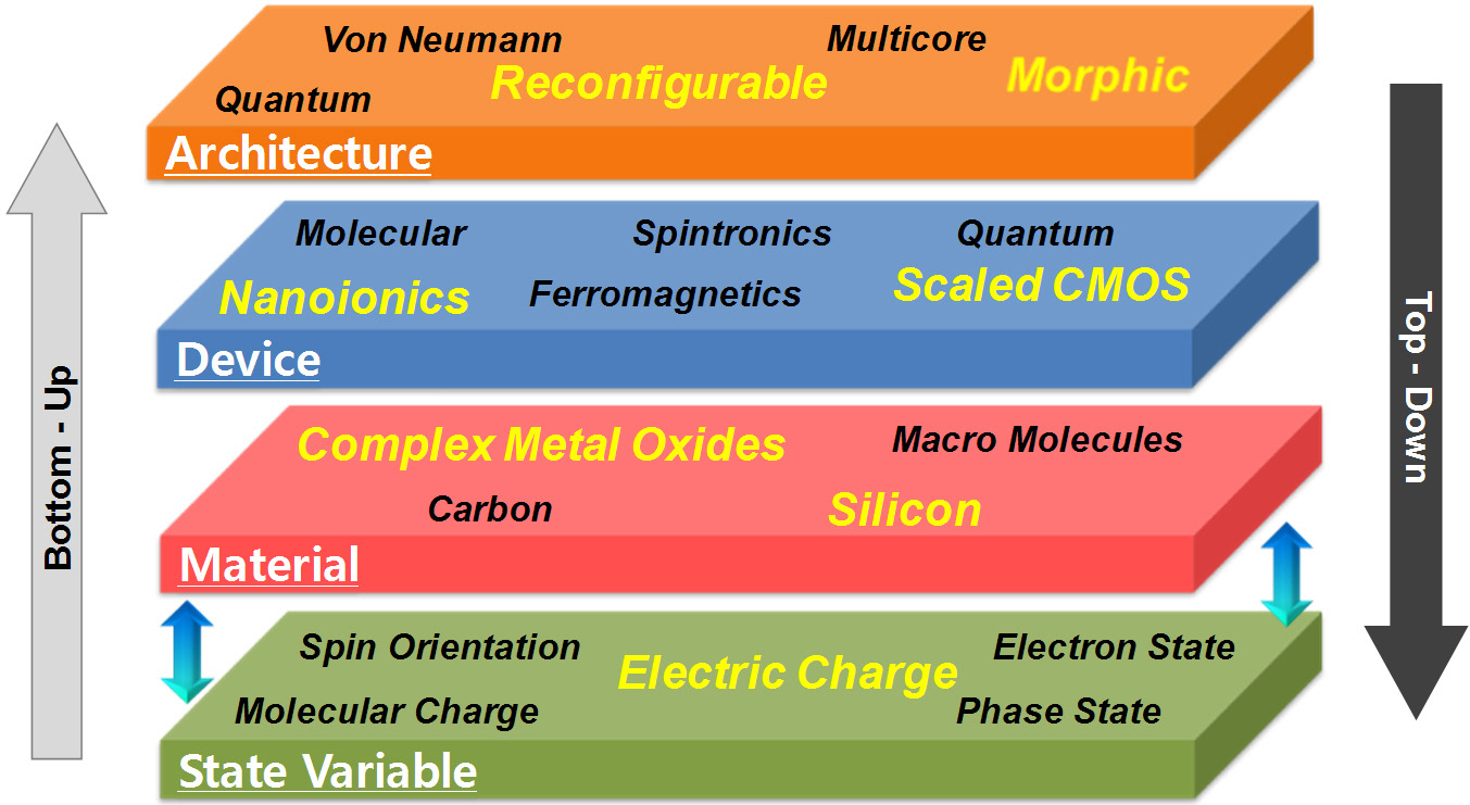
2. DESIGN DOMAINS AND TECHNOLOGIES
Future of information technology is very much dependent upon formulation of new materials and realization of device concepts that allow for improved functionality and are economically scalable. The spectrum of activities towards enhancements to silicon technology with the promise of extension of its life cycle has paved the way in implementation of novel approaches. These include by the way of an example, replacement of silicon channel and possibly the source/drain regions with new kind of materials such as graphene and graphene nanoribbons, carbon nanotubes, and incorporation of III-V and Ge semiconductors that offer a higher quasi-ballistic-carrier velocity and higher mobility. Such innovations are conjectured to move the performance of scaled silicon devices beyond 16 nm regimes [7]. As the consequence two frontiers of research are being pursued simul-
taneously.These are: (a) integration of heterogeneous technologies to extend the CMOS performance platform, (b) formulation of new information processing concepts in the realization of new logic devices leading to new nanoarchitectures that if successful will extend substantially the technology Roadmap way beyond current projections [7].
The integrated circuit industry is accustomed to work within the ‘Old Science’ framework where structures are machined to shape as is the case with the
3. MEMORY: THE PACE SETTER FOR NANO-ARCHITECTURES
The memory technology has been the pace setter and has driven the semiconductor platform as the enabler of new and novel architectures. Invariably the experiences gained in scal-
ing of the technology have influenced the realization of new generation of circuits and systems. Thus far because of the high density and low fabrication costs, the silicon-based Flash has continued as the front runner of NVM applications. However both Flash and static random access memory (SRAM) are likely to reach their fundamental limits sometimes around 2016. As the consequence a kaleidoscope of activities have surrounded the development of new NVM devices that range from chalcogenide phase-change memory, ferromagnetic memory through to new structures based on transition-metal-oxides that can be conditioned to exhibit bi-stable behavior [8, 9].
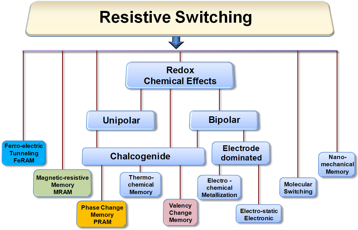
Over the last half century the quest for a universal memory (UM) has challenged both researchers and industry. Thus far very few memory based research programs have yield practical devices that could be said are likely to under-pin future micro and nanoarchitectures satisfying the needs of intelligent integrated SoS (i2SoS) taxonomy. With rapid progress in material science and the anticipated changes that appear on the horizon, it is sensible to review some of the more salient features of the NVM technology and the research practices being driven by different fundamental mechanisms such as polarization of ferroelectric gate dielectric, electronic charge encapsulated within dielectric, and resistive state changes as the result of either electric or magnetic perturbations. Figure 2 provides a generic summary of NVM approaches based on chemical, thermal, magnetic and electronic charge switching effects which promise new and unexpected functionalities. Combination of these memory devices with the silicon CMOS most likely will pave its way into diverse applications such as content addressable memory (CAM) used in search engines where digital search data forms the basic data construct, through to emulation of neurons and synaptic elements in neuromorphic circuits where analog processing and learning in the form of past history create the computational framework [10,11].
3.1.1 Ferroelectric RAM
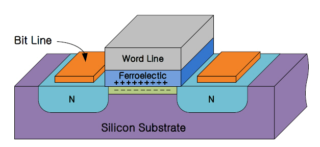
Ferroelectric RAM (FeRAM) cell shown in Fig. 3 is similar in construction to that of the widely used dynamic RAM (DRAM) storage cell which consists of an access transistor and a capacitor-based storage node. In FeRAM, ferroelectric material such as lead zinconate titanate (PZT) is used as the dielectric that forms a ferroelectric capacitor integrated into the body of the gate of the transistor. The nonlinear relationship that exists between an applied electric field E and the stored charge q is the mechanism that provides the hysteresis effect that facilitates storage [12].
The dielectric constant in Fe capacitor that forms the FeRAM cell is much higher than the linear dielectric used in conventional MOS. Such characteristics are the result of formation of semipermanent electric dipoles in the crystal lattice. ‘Writing’ takes place upon application of an electric field E across the ferroelectric layer whereby the dipoles align themselves in the direction of the field, creating small shifts in the positions of atoms, thus forcing a change in the distributions of electronic charge q in the crystal structure. When the applied field is removed the dipoles continue to retain their polarization state. ‘Reading’ is accomplished by the reorientation of the atoms in the dielectric. As electrons are pushed out of the metal, a short current pulse on the Bit Line signals the state of the memory cell. Power is only needed during the reading and the writing cycles. Inclusion of PZT layer and the noble metals necessary for electrodes as part of CMOS processing introduce a number of compatibility issues due to contamination. Scaling also remains a problem and there appears to be no simple solution as yet to alleviate the material complexity. However, more recent developments using graphene, nanowires and organic ferroelectrics have provided new possibilities in addressing the overall reliability issues and hence FeRAM’s viability in future products [13].
3.1.2 Phase change memory
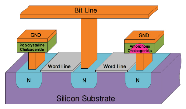
Phase-change memory (PRAM) shown in Fig. 4 dates back to 1960’s when Stanford R. Ovshisky experimented with chalcogenide glass after noting that the electrical resistivity of amorphous and crystalline states were significantly different which meant it could be considered as a candidate for data storage. PRAM which is also referred to as chalcogenide RAM, phase change memory (PCM) and PCRAM, is based on the intrinsic behavior of the alloy of chalcogenide glass-germanium, antimony and tellurium (GeSbTe)-that exhibits switching between the two states: ‘crystalline’ corresponding to ‘ON’ state and ‘amorphous’ corresponding to ‘OFF’ state upon application of heat[14,15].The phase change memory mechanism is the result of filament growth by an inducing electric field. Better control of material has enabled realization of four distinct states, with each state having different electrical characteristic that corresponds not only to the previous amorphic and crystalline states, but also two additional partially crystalline states. This means a single cell can represent two bits of data, hence doubling the storage capacity. There remain a number of challenges for PRAM to be resolved. The rather large current density during programming phase-which can be up to two orders of magnitude greater than the corresponding scaled MOS transistor, has to be better managed. Furthermore, the long-term stability of amorphous resistance states and the related threshold voltage drift that follow the power law ~t0.1, slowly
increases with time and therefore has to be stabilized [16].
Nanothermal memory cell development has also attracted attention where the function is similar to PCM, but the cell construct is based on nanowire. The nanowire-structure phase change cell reduces the switching current during ‘Write’ operation [17,18] and therefore facilitates in resolving the material problems.
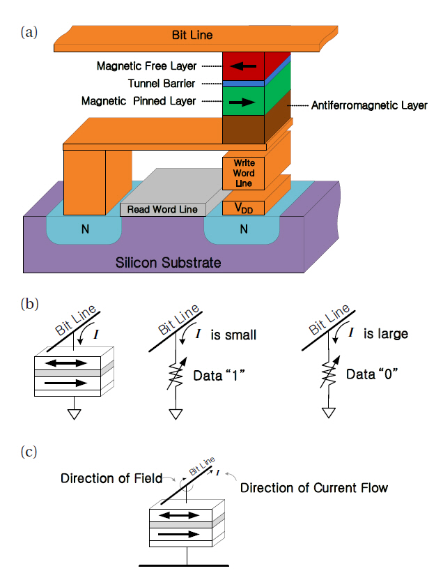
3.1.3 Magnetoresistive RAM
Magnetic storage forms the bases for magnetoresistive RAM (MRAM). Data is stored by intersection of two ferromagnetic wires-one of which is a permanent magnet and is set to a particular polarity. The MRAM structure consists of a grid of magnetic tunneling junctions. In contrast with conventional memories such as DRAM or SRAM where data is stored as electric charge q, in MRAM the storage mechanism occurs by perturbation to magnetic field forming the cell. When current travels through a line that opposes the polarization of one of the magnetic field bits, its current is mitigated and the data stored by the field is detected. A simplified physical construct of the cell together with ‘Read’ and ‘Write’ operations are shown in Fig. 5. The two wires shown in Fig. 5 are separated by a thin insulating dielectric layer and hold a magnetic field. In order to store data-namely the read cycle-the field on one wire is changed to match that of an external field. Several approaches are pursued in ‘Writing’ data to the cells. In one approach, each cell is organized between a pair of ‘Write’ lines-located above and below the cell-arranged at right angles to each other. When current flows in the lines, an induced magnetic field is created at the junction, which the ‘Write’ line detects. The main disadvantage of such an approach is the requirement for relatively substantial amount of current to create the threshold field required during the writing phase. A further problem is the false writes that may occur as the consequence of scaling of the technology [19,20].
3.1.4 Resistor RAM
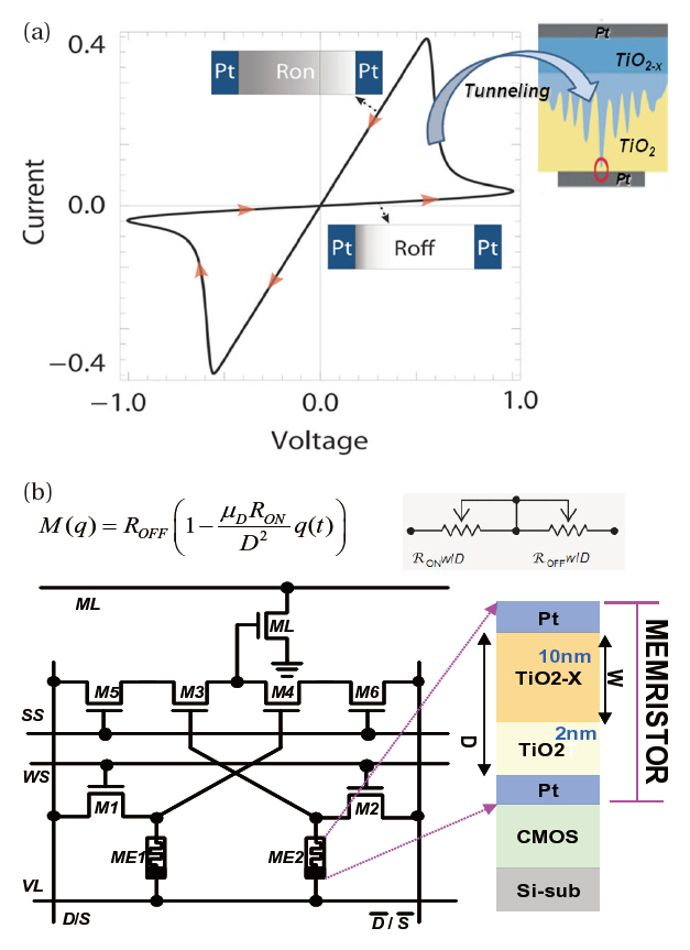
Experimentation with materials having ‘history-dependence’ in device constructs at nanoscales has created renewed interests in resistance-change memory (RRAM) which is also referred to as Memristor, a concept postulated by Chua in 1971 as the fourth fundamental circuit element [21-23] due to the expected symmetry between resistor R, capacitor C and inductor L. Chua’s Memristor can be constructed in the form of a metal-insulator-metal (MIM) construct composed of transition-metal-oxides such as Titanium dioxide (TiO2) layer sandwiched between two conducting plates as shown in Fig. 6 [24]. TiO2 changes its resistance when oxygen is present. The plates maybe composed of a variety
of different conducting materials such as Pt, Ag and ITO. The movements of ions in the layer are related to the motion of electrons in the material which in turn permit a state change in the atomic structure of the MIM cell. As the consequence the cell exhibits a resistance state switching (bitable) when a programming voltage
There are a number of newly engineered materials under investigations. These include ZrO2, WO3, Ir2O3, MoO3 and RhO2 which also have shown memristive properties. Variations based on CuO, NiO, ZrO, and HfO materials have also been under experimental evaluation. Perovskite materials are based on a vari-
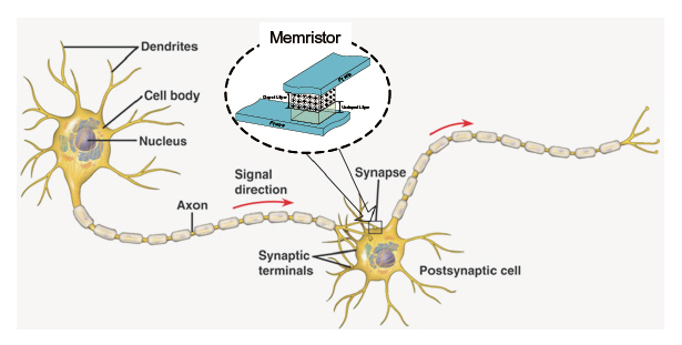
ety of Ternary Oxides such as SrTiO3, SrZrO3, BaTiO3 and PCMO. These materials appear to have variable resistances which are more easily tunable and in addition have exhibited capacitive hysteresis effect. As the consequence this novel characteristic will influence the manner in which logic is designed to conserve energy. Perhaps the important issue to be considered is that whatever kind of materials used they need to be compatible with CMOS processing in order to gain an economic advantage in both near and the mid-range future. Application of Memristor as part a heterogeneous architecture in the design of Memristorbased content addressable memory (MCAM) for the resource intensive search engines is shown in Fig. 6(b). The MCAM cell offers some 90% reduction in power consumption highlighting the scope and significance of the technology. Other applications of Memristor are highly compatible with neuromorphic design taxonomy. Neural networks learn patterns that are based on an analog memory element. Chua’s equations for the Memristor are similar in form to that of the Hodgkin-Huxley model that describes the behavior of neural cells [25,26]. Memristor integrates both the memory function and signal processing-much similar to neural synapses-and therefore can mimic biological architectures. Learning occurs when simultaneous voltage spikes are generated from edge detectors such as those encountered in biological systems namely the eye or the touch. Receiving synapse in the brain responds to the incoming stimuli by increasing its threshold value. Memristor are ideal for realization of a synthetic based architecture similar to that of the human brain capable
of handling applications such as pattern recognition and selections,adaptive control etc. A simplified view for implementation of a Memristor as part of neural cell is shown in Fig. 7.
3.1.5 Spin transfer torque memory
Spin transfer switching or spin transfer torque memory (STTRAM) is an advanced version of MRAM currently being pursued.The approach is based on the degree of freedom in electron spin and the related electron spin polarization. It is a kind of
Electrons that flow in a device carry charge q having spins. In non-ferromagnetic materials the electron spins are random and do not have a function in characterizing the behavior of the material as such. However introduction of ferromagnetic material forces the flow of electron charge to become spin-polarized and hence alters the characteristic of the material. The interaction that takes place between ferromagnets and electrons determine the magnitude of current available for detection of the internal state of STTRAM cell. In simplified form, the STTRAM cell is constructed from two ferromagnetic layers that are separated by a tunneling barrier layer such as MgO. Streams of electrons move through a magnetic material with a fixed orientation namely are being ‘spin-polarized.’ Usually the charge movement is not polarized, meaning it consists of 50% spin-up electrons and 50% spin-down electrons. However in the case of a spin-polarized current there will be more electrons having either of the two spin orientation. Switching of state then occurs as the result of the flow of spin-polarized electrons which are magnetized in the same direction as the magnet. The state is determined by the change in resistance of the cell. The ‘Read’ process is similar to that of MRAM. The ‘Write’ operation in STTRAM requires less energy-namely reduced writing current-thus providing improvement in scalability of the technology [27,28]. Since the coherent spin rotation of electrons does not dissipate energy, the technology promises an extremely low-power replacement for CMOS [29,30].
3.1.6 Progression of NVM developments
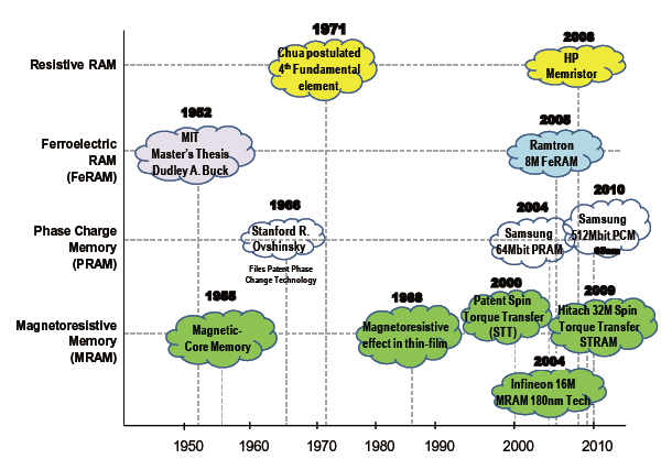
The scope and progression of NVM developments is shown in Fig. 8 which illustrates the innovations in material design and memory cells during the last half century. The range of available memories highlight the strengths as well as weaknesses when applied to different architectures.
In early 1980’s the doom of silicon MOS transistors was foreshadowed and scaling of the humble MOS transistors beyond 140 nm appeared as an impossible dream. However as it has turned out the emergence of new materials together with new techniques in lithography and processing have paved the way for a revised predication that has foreshadowed the feature sizes in the order of 16 nm will occur somewhere around 2016. Coupled with these developments, nanochemists have also began to probe into matter and now nanochemistry is beginning to shape the future of new materials as we better understand the unique properties of assemblies of atoms and molecules. Such progress supported by bio-based technologies provide the foundation for a future in which information sensing, embedded processing,imaging and multi-level communication become pervasive. Although a wide variety of systems exhibit memristive behavior,and as time progresses most likely new ones will be discovered as industry and academia become even more interested in the likely solution, the memory experience such as those gained through research programs involved with FeRAM, PRAM, MRAM, RRAM and related activities such as those of STTRAM have been rich and has provided new research options, that at this juncture it can be viewed as only an interim solution. Inevitably success will be measured by better performance (Read and Write times), cost, reliability, endurance, and life cycle of the product. The possibility of new architectures based on new materials is likely to challenge the perspective and the current mind-set that researchers and industry may have as we await the arrival of the universal memory.


![Resistive switching effects for non-volatile memories [10].](http://oak.go.kr/repository/journal/10323/E1TEAO_2010_v11n6_243_f002.jpg)