One of the flat panel displays, the organic light emitting device (OLED), is a spontaneous photon emission device. It offers a higher quality display than those of existing displays. Thanks to its simple manufacturing process, it is very competitive in price. Also, various advantages such as its wide viewing angle, good response speed, and thinness have highlighted the OLED as a next generation display that is superior to the liquid crystal display (LCD) and plasma display panel (PDP) [1, 2].
The OLED is a new type of light source known as a surface light source. The applications of OLEDs will be enlarged in the lighting market and the new e-paper market, as well as in the display market [3]. Tang and VanSlyke [4] studied a multi-layer OLED composed of an emission layer and a hole transport layer, which had been studied previously [5]. However, OLEDs have not yet achieved the long lifespans, high efficiency, high brightness, and high purity necessary for full-color realization [6].
There are various methods for realizing full-color OLEDs. The three-color separate emission method (driving separate pixels by separate emissions using three colors of red, green, and blue) and the white emission method (using white emission and color filters) have been researched [7, 8]. The white emission method can use the current LCD process lines and can be applied diversely in light sources, except in displays [9, 10]. The three peak white emission method mixes the three primary colors, and the two peaks white emission method mixes the blue (or bluishgreen) and red (or orange) colors [11]. The excellent performances of the two peak white emission method with regard to stability, efficiency, and process have been highlighted recently [12, 13] because it also has low color interference and easily controlled colors. Moreover, the manufacturing costs may be reduced as the control factors decrease [13].
Consequently, we improve the stabilities of white OLEDs through a structural change using the two peak emission method.
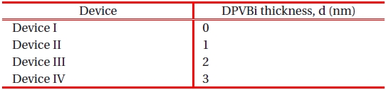
[Table 1.] Device structure thicknesses.

Device structure thicknesses.
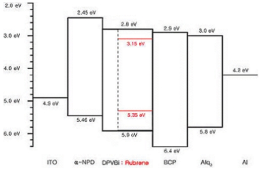
White OLEDs were fabricated on transparent indium tin oxide (ITO), which had a surface resistance of 10 Ω/□ and was coated onto a glass substrate. The patterned ITO substrate was cut into 1 inch 1 inch sections to be used as test pieces, which were essentially composed of ITO (100 nm)/ α-NPD (30 nm)/ 4,40-bis(2,20-diphenylvinyl)-1,10-biphenyl (DPVBi,
An orange light-emitting Rubrene was used as a dopant material, and the doping concentration was fixed at 2.0% (by weight). Alq3 was used to inject electrons easily into the EML. To bind the holes to the EML and restrict the electron-hole recombination zone to the EML, BCP was injected between the EML and the HTL to function as a hole blocking layer. Aluminum was used for the cathode electrode since it has a low work function and a strong anti-oxidation property in air. Each layer was vacuum evaporated at 5-10 nm/sec in the vacuum condition of 10-7 torr. The luminous properties of the fabricated devices were characterized, and their electrical properties were obtained. Figure 1 shows the energy-band diagram of the fabricated devices.
We focused on fabricating new white OLEDs using partially doped EMLs, which operate stably and can thus be used for lighting in the future. We obtained white color in two peak emission using the blue and orange EMLs.
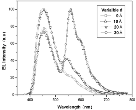
Figure 2 shows the electro-luminescence (EL) spectra for the different DPVBi thicknesses from the interface.
The applied voltage for each device was 14 V. The maximum values of the blue and orange EL spectra were normalized. In the case of device I (
As the thickness was increased from
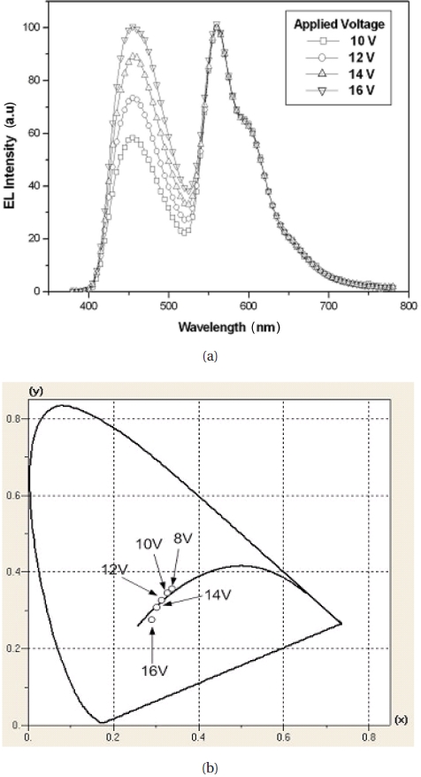
Figures 3(a) and (b) show the EL spectra and CIE coordinates of device I with a change in the applied voltage (
As shown in Fig. 3(a), in the case of increased voltage from 10 V to 16 V, yellow EL intensity was unchanged, but blue EL intensity increased. In Fig. 3(b), the transition of the CIE coordinates was shifted as well as the increased voltage. When the doping concentration was fixed at 2.0% (by weight) and a voltage of 12 V, a white emission with CIE coordinates of (0.3219, 0.3383) was close to that of pure white light (0.3333, 0.3333). Though it was revealed to have closer CIE coordinates to those of pure white light at 12 V-14 V, it shifted from a white light area to a blue light area at voltages greater than 16 V. At 19 V, the current density and the maximum external quantum efficiency were 128 mA/cm2 and 0.43%, respectively, and it had a maximum luminance of 184 cd/m2.
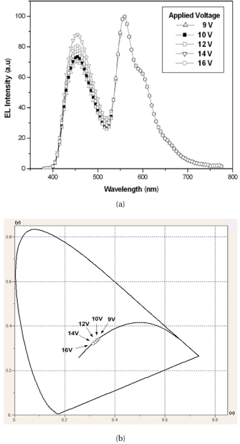
Figures 4(a) and (b) show the EL spectra and CIE coordinates of device II with a change in the applied voltage (
As shown in Fig. 4(a), in the case of a voltage increase from 10 V to 16 V, the yellow EL intensity was unchanged and the blue EL intensity was increased in the same manner as for device I in Fig. 3(a). However, the change in the blue EL intensity was not much greater than that in the case of Fig. 3(a).
As in Fig. 4(b), a white emission with CIE coordinates of (0.3342, 0.3439) was the closest to pure white light with CIE coordinates at 14 V. Judging from the CIE coordinates, it seemed that pure white light would be produced in the voltage range of 10 V-16 V.
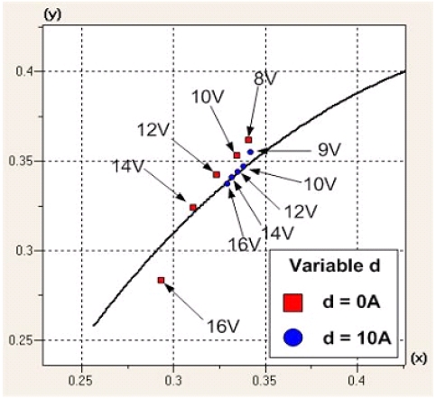
Figure 5 compares the white emissions of device I (
In the case of device II, the white emission area seemed totally insensitive to the drive voltages at 10 V-16 V compared to those of device I.
When the orange emitting Rubrene material was doped onto the emitting layer, the emission zone due to the energy transition was limited to within ~5 nm from the interface. The function of the Rubrene is to shallowly capture holes at a constant position away from the interface, and this position becomes a hopping site for the easy transmission of electrons. The Rubrene also improves the mobility of the electrons and captures electrons while maintaining a proper distance from the interface. As a result, early saturation of the recombination site is prevented so that the site can be stably recombined. Therefore, it was identified that the EL spectra and CIE coordinates were insensitive to the drive voltage.
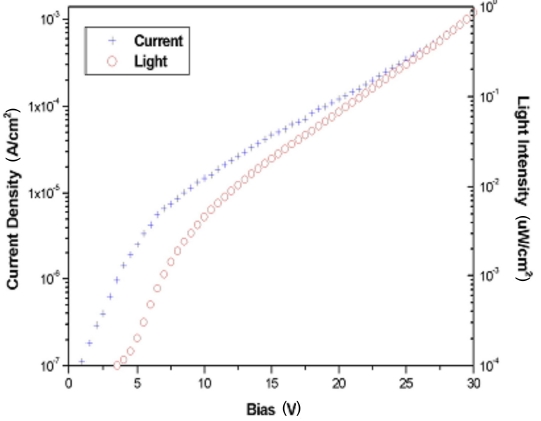
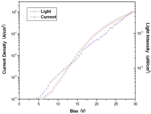
Figure 6 shows the current-voltage-light intensity characteristics of device 1.
In Fig. 6, the operating and emission states were 2 V and 4 V, respectively. As the voltage increased, the light intensity increased rapidly, starting at 5 V. This is because energy was transmitted from the Rubrene at less than 12 V, and orange emission appeared predominately.
This is the same reason that, in the CIE coordinates, the orange emission predominately appeared at low voltages and the blue emission predominately appeared at high voltages, with a maximum luminance of 184 cd/m2. At 19 V, the current density and the maximum external quantum efficiency were 128 mA/cm2 and 0.43% respectively. The external quantum efficiency slowed incrementally from 15 V and decreased from 19 V, explaining why, as the voltage increased, the number of excitons disappearing without emission due to the saturation of the photons increased. Thus, the light intensity increases more slowly than does the current density.
Figure 7 shows the current-voltage-light intensity characteristics of device II, in which the operating and emission state voltages were 4.5 V and 5.5 V, respectively. The light intensity was slightly higher than in the case of device I. On this account, the initial orange emission by the Rubrene on the interface is weak. This shows that the light intensity was steadily increased without rapid increase or decrease to the drive voltage. This also was identified in the CIE coordinates and EL spectra, in which there was insensitivity to the drive voltage. Device II had a maximum luminance of 211 cd/m2, and, at 19 V, the current density and the maximum external quantum efficiency were 173 mA/cm2 and 0.478% respectively. The maximum luminance and the external quantum efficiency were greater than in the case of device I.
White OLEDs utilizing the two peak white emission method using blue EML and orange EML were fabricated. The fabricated devices are composed of ITO (100 nm)/ α-NPD (30 nm)/ DPVBi (