One-dimensional porous TiO2 nanotube structures have received great attentions for applications in photovoltaics [1-5], gas sensors [6], electrochromic devices [7], Li-secondary batteries [8], etc. TiO2 nanotubes have been fabricated by various methods such as deposition into a nanoporous alumina template [9], solgel transcription using organo-gelators as templates [10], seeded growth [11], hydrothermal processes [12], and anodization processes [13,14]. Highly ordered TiO2 nanotube arrays, which have by far the most remarkable properties, can be made by anodic oxidation of titanium in fluoride-based baths [15].
Electrolyte composition and its pH determine both the rate of nanotube formation and the rate at which the resultant oxide is dissolved. Several aqueous electrolytes such as HF/H2O [13], H2O4/H2O [16], HF-CrO4/H2O [17], and KF/NaF/H2O [18] have recently been used to create TiO2 nanotube arrays. However, there is a limitation to increase the thickness of TiO2 nanotube arrays in aqueous electrolyte solution due to the vigorous chemical dissolution of the oxide by fluorine ions [15]. With organic electrolytes, the donation of oxygen is more difficult compared to water, thus reducing the tendency to form oxide. At the same time, the reduction in water content reduces the chemical dissolution of the oxide in the fluorine containing electrolytes and hence aids the longer-nanotube formation [15]. These organic electrolytes include dimethyl sulfoxide, formamide, ethylene glycol, and N-methylformamide [19]. Paulose et al. [20] fabricated mechanically stable TiO2 nanotube arrays up to 1,000 μm in length by using ethylene glycol electrolyte containing 0.6 wt?% NH4F and 3.5 vol?% H2O.
In this study, we prepared TiO2 nanotube arrays by anodic oxidation of Ti metal in ethylene glycol solution. Several properties of TiO2 nanotube arrays such as crystal structure, morphology, current-time behavior during anodization, etc., were studied.
Highly ordered TiO2 nanotube arrays were fabricated by anodic oxidation of 0.5 mm thick Ti foil (99.0%, Alfar Aesar, Word Hill, Massachusetts, USA) at a constant potential 60 V (ramping up to 60 V with a ramping speed 1 V/s) in the ethylene glycol solution containing 0.3 wt?% NH4F and 2 vol?% H2O. The anodized samples were annealed at 500℃ for 60 minutes to crystallize the amor-phous TiO2 nanotube arrays. Pt metal was used as a counter electrode. The anodization voltage was applied by a DC power supply (Model XKW600-1.7, Xantrex Technology, Inc., Burnaby, Canada). Current-transient curve was measured during anodization using a digital multimeter (Model 34401A, Agilent Technologies, Inc., Santa Clara, CA, USA) interfaced with a computer. Power supply and multimeter were computer-controlled with GPIB interface and LabVIEW program (National Instrument, Austin, TX, USA).
The length, pore size, diameter, and wall thickness of TiO2 nanotube arrays were determined by field emission scanning electron microscopy (FESEM, Philips XL 30SFEG; Philips, Amsterdam, Netherlands) analysis. Crystal properties of TiO2 nanotube arrays were studied by X-ray diffractometry (XRD, Rigaku D/ MAX-RC, CuKa radiation; Rigaku, Tokyo, Japan) and field emission transmission electron microscopy (FETEM, Tecnai G2 F30 S-TWIN; FEI, Hilsboro, OR, USA) analysis. X-ray photoelectron spectroscopy (XPS, Thermo VG Scientific ESCA 2000; Thermo Fisher Scientific, Waltham, MA, USA) analysis was introduced to study the chemical composition and the bonding energy of Ti and O ions in crystallized TiO2 nanotube arrays.
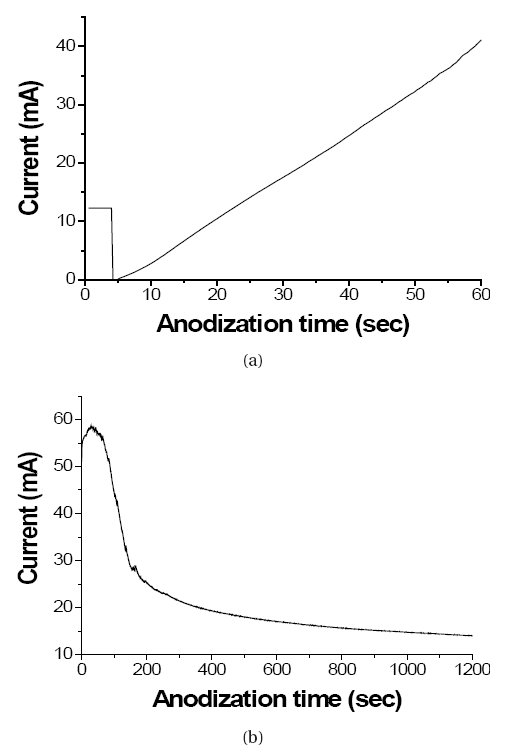
Figure 1 shows current-transient curves obtained during anodic oxidation of Ti foil. Figure 1(a) gives the current-time behavior when the anodization voltage increases from 0 V to 60 V at the ramping speed of 1 V/s. In the early stage of voltage ramping, the current, which flows from Ti anode to Pt cathode, abruptly decreases due to the formation of thin TiO2 layer on Ti foil. However, after ~4 seconds, the current increases in proportion to the ramping time. It seems that the as-formed TiO2 layer on Ti foil is not thick enough to block the current flow thus the current is proportional to the ramping voltage.
A current-transient curve obtained at a constant voltage of 60 V during anodizing process can be shown in Fig. 1(b). At the beginning the current increases to some extent because etching of thin TiO2 layer on Ti foil by F ions exposes Ti metal. However, the exposed surface of Ti metal is readily converted to thin TiO2 layer thus the current decreases according to the anodizing time. TiO2 nanotube structures start to be formed from the moment at which the current decreases. Directional etching of TiO2 and Ti by F- ions induced by an applied voltage makes possible to fabricate highly ordered TiO2 nanotube arrays.
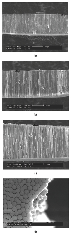
Figure 2 shows FESEM images of TiO2 nanotube arrays obtained by anodic oxidation of Ti foil in 0.3 wt?% NH4F contained ethylene glycol solution. Figures 2(a)-(c) give the cross-section images obtained by anodization at a constant voltage of 60 V for 20, 30, and 40 minutes, respectively. The thickness of TiO2 nanotube arrays increased from 18 μm for 20 minutes anodization to 30.8 μm for 40 minutes anodization. In ethylene glycol solution, the movement of F- ions is slow thus the etching speed for the surface of TiO2 nanotube arrays is lower than that in aqueous solution [15, 19, 20]. Longer nanotube arrays up to 1,000 μm can be obtained by controlling NH4F concentration, anodizing time, anodizing voltage, etc. [20]. The bottom and cross-section images of TiO2 nanotube arrays can be shown in Fig. 2(d). TiO2 nanotube arrays were close-packed together and the bottom of each TiO2 nanotube was blocked. The diameter, wall thickness, pore size of each TiO2 nanotube were ~120 nm, ~40 nm, ~40 nm, respectively.
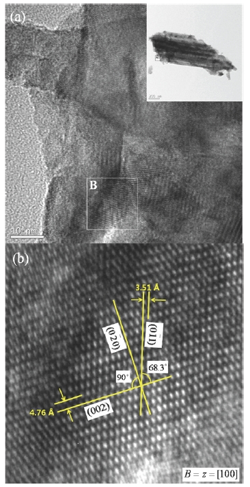
Figure 3 shows FETEM images of annealed TiO2 nanotube arrays. Figure 3(a) is the magnified image of part A in the inset figure and Fig. 3(b) gives the magnified image of part B in Fig. 3(a). There are several crystal fringes in Fig. 3(a) and each fringe has a different orientation. From these results, we can know that the annealed TiO2 nanotube arrays have a polycrystalline structure which is composed of several crystal grains. It seems that each fringe represents a TiO2 single-crystal grain. Ordered arrays of Ti and O atoms in annealed TiO2 nanotube arrays are shown in Fig. 3(b). The high resolution TEM image (Fig. 3(b)) shows (01), (0~0), and (002) atomic planes with a diffraction direction of z axis [100] zone. The interfacial angle of (01) and (002) is 68.3oC and that of (0~0) and (002) is 90oC. Lattice spaces of (01) and (002) are 3.51 A and 4.76 A, respectively. These values of interfacial angles and lattice spaces are identical to theoretical values of anatase TiO2 crystal structure [21].
The as-anodized TiO2 nantoube arrays have an amorphous structure (data not shown here). After heat treatment at 500℃ for 1 hour, the amorphous TiO2 nanotube arrays are converted to anatase polycrytalline structure. It can be shown from the results of FETEM analysis that anatase phase of TiO2 nanotube arrays could be successfully formed by heat treatment.
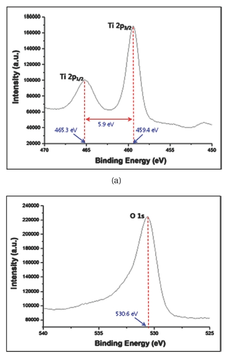
Figure 4 shows XPS results of annealed TiO2 nanotube arrays. Three characteristic peaks of Ti and O can be observed in Figs. 4(a) and (b). The binding energies of Ti 2p1/2, Ti 2p3/2, and O 1s peaks are 465.3 eV, 459.4 eV, and 530.6 eV, respectively. The difference of binding energies of Ti 2p1/2 and Ti 2p3/2 can be seen as 5.9 eV in Fig. 4(a). This means that Ti has a tetravalent state in TiO2 nanotube arrays [22]. The measured binding energies of 465.3 eV for the Ti 2p1/2 peak, 459.4 eV for the Ti 2p3/2 peak, and 530.6 eV for the O 1s peak are in excellent agreement with the previously published results of anatase TiO2 crystal structure [22,23].
Highly ordered TiO2 nanotube arrays were fabricated by using anodization process. As-anodized TiO2 nanotube arrays had an amorphous structure. After heat treatment of as-anodized samples, anatase phase of TiO2 nanotube arrays could be obtained. FESEM analysis showed the successful formation of highly ordered TiO2 nanotube arrays by anodic oxidation of Ti foil. We could confirm the conversion of crystal phase of TiO2 nanotube arrays from amorphous to anatase crystalline by FETEM and XPS.