Recently, transparent conductive oxide (TCO) thin films have been used in a variety of electrical and optical applications such as light-emitting diodes (LEDs), solar cells, displays, and so on. Al-doped ZnO (AZO) is emerging as an alternative candidate for indium tin oxide (ITO) films due to its cheapness, remarkable electrical conductivity, the chemical stability lacking in ITO, abundant raw materials, and nontoxic features. It is easy to fabricate as well [1].
When AZO thin films are used as an electrical contact and window layer for GaAs/GaAlAs LEDs, they need to have high transmission capabilities at the wavelength of 940 nm (T ≥ 80%) and a low resistivity (ρ ≤ 10-3 Ω.cm) [2]. It is difficult to obtain reproducible AZO thin films with these suitable properties at a low deposition temperature. However, a high deposition temperature may damage the substrate or device.
Thermally treated AZO films in hydrogen ambient exhibit an enhanced electrical conductivity. In the case of ZnO films, the effect of hydrogen on the changes in the electrical characteristics of the films has been studied in detail [3,4]. According to these recent works, the electron concentration of the ZnO films increased, since hydrogen atoms were incorporated between the Zn-O bonds by the mixing of Ar and H2 ambient, which formed shallow donor levels. It is also known that the hydrogen removes the negatively charged oxygen species on the surface of the ZnO films by thermal treatment in hydrogen ambient, resulting in the increase of carrier mobility [5]. However, the long-term stability in the electrical characteristics and the origin of the enhanced electrical conductivity of the hydrogen-annealed AZO films used for transparent electrode applications have not been established yet.
In this paper, AZO thin films were deposited at the low temperature of 100℃. The introduction of H2 to the process of deposition was carried out to obtain a low resistivity and a high transmission. The structural, electrical and optical properties of the films with respect to the annealing temperature (300℃) in ambient atmospheric hydrogen for 1 hour were examined. The experiment revealed that AZO films with a low resistivity can be obtained at a low growth temperature in an Ar:H2 gas RF magnetron sputtering system [6].
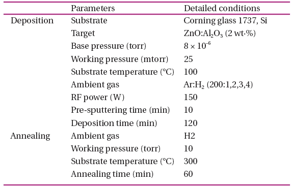
The conditions of the AZO thin film deposition on glass substrates by Ar:H2 gas RF magnetron sputtering and annealing.
The AZO thin films were deposited on Corning 1737 glass, Si substrates at the base-pressure of 25 mtorr and a temperature of 100℃ by the Ar:H2 gas radio frequency (RF) magnetron sputtering system using an AZO (2 wt.% Al2O3) ceramic target. The substrates were ultrasonically cleaned sequentially in acetone, alcohol and de-ionized water, and then dried with nitrogen gas. The H2/Ar percentage was varied from 0.5% to 2%. The chamber was evacuated to 8 × 10⁻⁶ torr and the pre-sputtering time was 10 minutes. The RF power and deposition time were 150 W and 2 hours. The other conditions were the same for the AZO thin films. The annealing treatments were carried out in ambient atmospheric hydrogen for 1hr at a temperature of 300℃.
The influence of the hydrogen on the crystallinity of the films was investigated by X-ray diffraction (XRD) and scanning electron microscopy. The resistivity, mobility and carrier concentration were measured using the Hall effect in a Van der Pauw configuration. A spectrophotometer was used for measuring the transmittances of the AZO thin films in the wavelength range of 300-1,100 nm. The details of the deposition and annealing conditions for the AZO thin films are listed in Table 1.
3.1 The micro structural properties
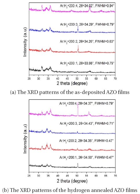
The XRD results are shown in Fig. 1. The XRD patterns of the as-deposited and hydrogen annealed AZO films are exhibited around the (002) peak of the standard ZnO crystal (2 θ =34.33o), indicating that the films have a c-axis preferred orientation due to the self-texturing phenomenon [7]. The (002) peak in the ZnO crystals had the lowest surface energy, so that the continuous films tend to change into (002) orientation films to minimize the surface energy [8]. The corresponding diffraction angle of the films prepared in the Ar:H2 mixed gas is smaller than that in the Ar gas, implying that the crystal c-axis of the film grown in the mixture of hydrogen was expanded [9]. This effect is due to the hydrogen atoms situated in the Zn-O bond center, making the lattice c-axis constant of the films increase. After annealing at 300℃ for 1 hour in hydrogen gas, it can be implied that the average grain size decreases according to the Scherrer formula [10]. The position of the (002) diffraction peak of the films grown in the Ar:H2 mixed gas increases after annealing at 300℃ for 1 hour in hydrogen gas. The Debye-Scherrer equation also supports the idea that the AZO films had a large surface area in the grain boundaries and the surface states of the grain possibly affect the electrical characteristics of the films. Lin et al. [11] also reported that, according to XRD analysis, most of the Al atoms were not in a ZnO crystalline state when the chamber had only Ar gas. Thus, it can be concluded that hydrogen improves the efficiency of the substitution and makes more Al atoms sit in the site of the Zn atoms compared to the films deposited under a pure Ar ambient. As a result, the number of impurities at the grain boundaries decreases, allowing the grain size to become bigger [12]. The full-width at half-maximum (FWHM) of the hydrogen- annealed films is smaller than that in the as-deposited films, implying that the hydrogen is beneficial to large grain formation. The position of the (002) peak shifts to the right after annealing. This suggests a relaxation of the residual tensile strain introduced in the films during the depositing process [13], indicating that as the H2 flow ratio changes the grain size changed.
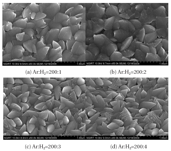
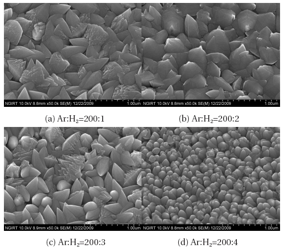
Figures 2 and 3 show the surface morphologies of the asdeposited and the hydrogen-annealed films. After the annealing process, the morphology of the films deposited in the Ar:H2 mixed gas becomes more compact and structured.
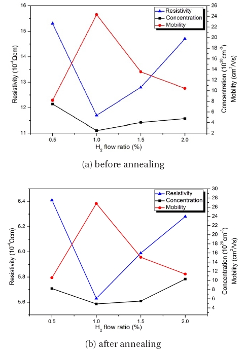
Figure 4 shows the influence of the H2 flow ratio on the electrical properties before and after annealing in the hydrogen atmosphere. Among the films deposited in the Ar:H2 gas RF magnetron sputtering system, the best resistivity is 11.7 × 10⁻⁴ Ω.cm in the film deposited with the H2 flow ratio of 1%. After annealing, the results show the resistance decreases in all of the films. The lowest resistivity is 5.63 × 10⁻⁴ Ω.cm in the film deposited with the H2 flow ratio of 1%. The corresponding mobility increases from 24.32 cm2/Vs to 26.8 cm2/Vs and the carrier concentration increases from 2.49 × 1020 cm-3 to 4.87 × 1020 cm-3 in the film deposited with the H2 flow ratio of 1%. The main reason for this increase of mobility and carrier concentration is attributed to the desorption of the negatively charge oxygen species from the grain boundaries during the hydrogen annealing treatment. This suggests that the oxygen can make the resistivity increase [6,16]. This is represented by the following:
O- + H2 = H2O (g) + e
Therefore, it was concluded that the enhanced electrical characteristics of the hydrogen-annealed AZO films were induced by the increased carrier concentration and mobility due to the elimination of the adsorbed oxygen species by the hydrogenannealing treatment.
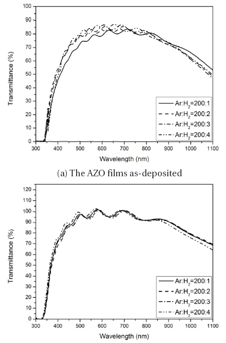
Figure 5 shows the transmission spectra of the AZO films prepared with different amounts of H2-flux. The samples were deposited with H2-flux ranging from 0.5% to 2%. The average transmittance in the range of 940 nm was 70% for all the films. After annealing, the average transmittance in the range of 940 nm was 85%, and the best transmittance of 86.5% was achieved for the film deposited with the H2 flow ratio of 1%. The absorption edge of the films shifted to the shorter wavelength region with the increasing H2 flow, which was due to the Fermi level moving into the conduction band with the increase of the carrier concentration, according to the theory of the Burstein-Moss effect [14,15]. This theory states that the optical band gap is widened with an increase in the donor concentration due to the filling of the conduction band by the increase of the electron carriers.
It was also found that the sample prepared with the H2 flow of 2% shows a slightly bad transparency in the visible region, which is a result from the intergranular zinc atoms due to the extraction of the O from the AZO films by excessive H. It is clear that the H2 played a significant role in determining the structural, electrical and optical properties in the case of the AZO film. Therefore, it can be concluded that the H2 flow ratio must be controlled to a moderate level in order to reduce the resistivity without being detrimental to the transmittance of the AZO thin films by the introduction of hydrogen [1].
AZO thin films with a low resistivity and high transmittance were deposited by an Ar:H2 gas RF magnetron sputtering system using a ZnO target mixed with 2 wt.% Al2O3 at the low temperature of 100℃. All the thin films exhibit a c-axis (002), oriented normal to the substrate. The structural, electrical and optical properties of the AZO films prepared with different H2 flow ratios were characterized. The electrical properties were enhanced due to the removal of the absorbed oxygen species at the grain boundaries by the hydrogen annealing process. The resistivity decreased from 11.7 × 10⁻⁴ Ω.cm to 5.63 × 10⁻⁴ Ω.cm after annealing in a hydrogen atmosphere for 1 hour at 300℃. We obtained the lowest resistivity by adding 1% hydrogen gas to the deposition and the annealing process. The average optical transmittance for all the films was 85% at 940 nm for the GaAs/GaAlAs LEDs. These results showed that H2 has a strong influence on the properties of AZO films.