Chalcopyrite Copper indium disulfide (CuInS2) thin films are the most promising materials for thin film photovoltaic devices due to their energy band gap of 1.5 eV which perfectly matches the solar spectrum for energy conversion. There is a strong demand for renewable energy due to the limited availability of fossil and nuclear fuels and growing environmental problems. Photovoltaic energy conversion has the potential to contribute significantly to the next generation of electrical energy [6]. CuInS2 is the focus of strong research interest among the materials suitable for thin film solar cells, such as amorphous silicon, CdTe and Cu(In,Ga)Se2 [7]. Cu-chalcopyrite semiconductor materials are used as absorber layers in heterojunction solar cell devices.
Polycrystalline solar cells with a Cu(In,Ga)Se2 absorber recently achieved conversion efficiencies of up to 18.8% [8]. Single phase CuInS2 thin film with a chalcopyrite structure has achieved conversion efficiencies of 27∼32% as its direct energy band gap of about 1.5eV lies in the optimum solar energy conversion range [9]. CuInS2 is a Se-free compound from the chalcopyrite family and is suitable for solar cells due to its high optical absorption. The development of CuInS2 is attractive because the problematic selenium is substituted by non-toxic sulfur. The open circuit voltage of CuInS2 solar cells is theoretically higher (1.2 V) than that of Cu(In,Ga)Se2 cells. However, up to now the efficiency of CuInS2 solar cells has been limited by open circuit voltage, which is far below the theoretical value. The best conversion efficiency for polycrystalline CuInS2 cells reported so far is 12.7% [10,11]. Thermal evaporation as a method for thin film CuInS2 preparation is a good approach with respect to economic considerations. An important advantage of thermal evaporation as a method for thin film preparation is that films with a large area can be prepared without a vacuum using simple, low-cost equipment. CuInS2 thin film can be easily obtained by sulfurization of the Cu-In precursor. However, thermal evaporation Cu-In precursors with excellent morphology have not been obtained. Therefore, in this study related to the manufacture of CuInS2 ternary compound thin film, deposition was conduce using sputtering and evaporation methods, and the annealing with sulfurization process was used in the vacuum chamber, our intention being to obtain a single phase compound thin film. The performance of our study is also described below.
In this study for manufacturing CuInS2 ternary compound thin film, deposition was conducted using sputtering and evaporation methods, and the annealing with sulfurization process was used in the vacuum chamber (10-3 torr), with the intention of obtaining a single-phase compound thin film. Thus, varying several deposition factors and annealing conditions differently and then measuring the structural and electrical characteristics depending upon such variations derived the optimum process variables. In this experiment, Cu/In stack layers were deposited using the sputtering method, enabling us to expect a stronger adhesive force with a substrate, while S was deposited using the thermal evaporation method, enabling us to expect a stronger adhesive force with a substrate, while S was deposited using the thermal evaporation method because its low melting point prevents sputtering from being available. Since the sputtering rate and the electric conductivity of Cu is high, the DC sputtering method was used for the deposition thereof. Meanwhile, for the deposition of In, the RF sputtering method was used so that a more stable sputtering might be available. Also, the sputtering rate depending upon the DC/RF power was controlled so that the composition ratio of Cu versus In might be around 1:1, and the substrate temperature affecting the quality of the thin film was varied in the range of RT to 300℃ at intervals of 100℃ and the annealing temperature of the thin film was varied RT to 550℃ in intervals of 100℃.
The thickness of the fabricated CuInS2 thin film was about 1.5 μ;m, which was sufficient to obtain an absorption coefficient of more than 1×104 cm-1. Micro-structural studies were carried out by XRD (D/MAX-1200, Rigaku Co., Shibuya-Ku, Tokyo, Japan) and SEM (JSM-5400, Jeol Co., Akishima, Tokyo, Japan). The electrical properties were measured by a Hall Effect Measurement system (HL5500PC, Accent Optical Technology Co., Oregon, USA), and the optical absorbance was measured by a UV/VIS/ NIR Spectrophotometer (CARY 1, Varian Co., NY, USA).
3.1 Microstructure properties of CuInS2 thin films
A sputtering yield and a deposition rate are varied depending upon the ion energy, and the ion energy can be controlled by the accelerated voltage as applied.
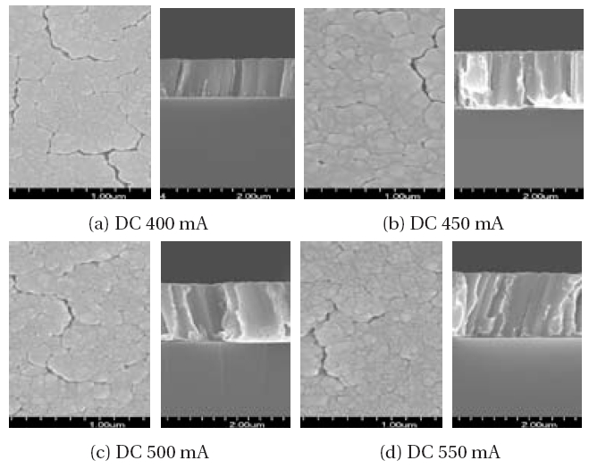
In order to investigate the depositing rate of Cu, the thickness and the surface configuration of the thin film, which was formed as DC power was varied in the range of 400 mA to 600 mA, were measured with scanning probe microscope (SPM) and FE-SEM, and the result shown in Fig. 1.
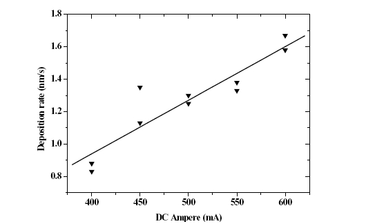
As shown in Fig. 1, it can be seen that they were almost linearly varied depending upon the DC power. This means, it is thought, that if DC power is increased, the energy of Ar ion incident upon the target becomes greater and leads to an increase in the sputtering yield and, consequently, the heat conductivity of In are lower than those of Cu, and RF power was used for the deposition thereof for the purpose of accomplishing a similar sputtering rate. Compared with the case where DC power was used, sputtering, which was substantially stable, could be available.
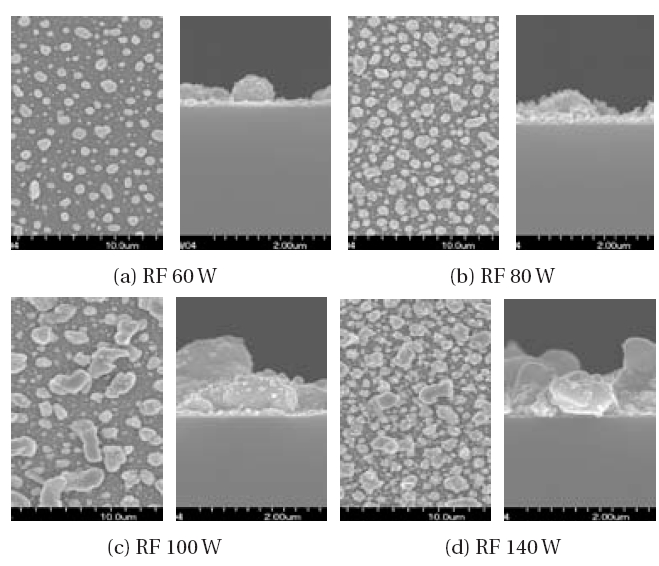
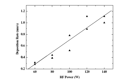
The depositing rate depending upon variation of RF power in the range of 60 W to 140 W is shown in Fig. 2, and it could be known that as RF power was increased, the depositing rate was almost linearly increased.
Each surface configuration of the thin film depending upon the deposing rate of Cu and In was measured with FE-SEM, and was shown in Figs. 3 and 4, respectively. Figure 3 represents a case where DC power was used to deposit Cu for 20 minutes, while Fig. 4 represents a case where RF power was used to deposit In for 30 minutes. It can be seen from the measurements of the thickness of the thin film with SPM and FE-SEM that, due to an increase in the thickness of the thin film, the size of the crystal grain is increased.
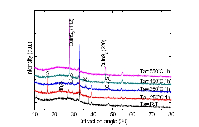
The diffract fringe of an X-ray, which depended upon the substrate temperature and the annealing temperature of the manufactured CuInS2 thin film, was investigated. Figure 5 represents a case where a sample manufactured at a substrate temperature of 200℃ was annealing temperature at R.T∼550℃. Until the annealing temperature rose to 350℃, second-order phases of CuS, Cu9In8, and In2S3 appeared, and at an annealing temperature of 450℃, such second-order phases disappeared and only the single phase of CuInS2 was observed. At a low annealing temperature of 250℃, the phase of Cu11In9, an excess of Cu appeared, and at annealing temperatures of 350℃ or higher, an excess of Cu disappeared and second-order phases of β -In2S3 and the like appeared.
This variation is consistent with the variation of the surface configuration at an annealing of 350℃. Such second-order phases did not appear at an annealing temperature of 450℃. In order to investigate this phenomenon more carefully, all samples manufactured at different substrate temperatures were annealing temperature of 450℃, and the results shown in Fig. 5. As expected, second-order phases were not observed at all, and only single phases of CuInS2 appeared.
3.2 Electrical properties of CuInS2 thin films
In order to examine the composition ratio of each element of CuInS2, the substrate temperature was varied in the range of RT to 200℃, and the annealing temperature was varied in the range of RT to 550℃ on the basis of the results of conducting the energy dispersive X-ray spectrometer (EDX) analysis and measuring the Hall effect to identify the conduction pattern, the carrier concentration and the Hall mobility thereof.
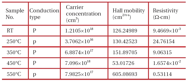
Electrical properties measurement of CuInS2 thin films after annealing at various temperatures.
As a result, p-type appeared. In order to analyze the cause of this result, an extent of an error beyond stoichiometry, which is represented by the value of ∇S, was obtained from the expression of ∇S = {2[S]/[Cu+3In]}-1. It is known that if its value is (+), p-type is available, while if its value is (-), n-type is available. Also, it can be seen from the experimental results that if the composition ratio of each element is appropriately adjusted, p-type or n-type can be artificially acquired. The object of this experiment is to acquire CuInS2 of n-type. The carrier concentration and the Hall mobility thereof are generally lower than those of CuInS2 of p-type, but it is thought that there will be no difficulty in using it as an absorption layer.
However, at an annealing temperature of 250℃ or lower, no compound is formed at all. This has also been identified through the SEM photo. In order to examine a relation between the composition ratio thereof at an annealing temperature of 350℃ or higher and the electrical characteristics thereof, the Hall Effect was measured and the result was shown in Table 1.
Both samples almost have the stoichiometric composition. It can be seen that as its composition gets closer to the stoichiometric composition, the p-type is more strongly shown. It was also identified that in order to show the n-type clearly in the condition of an annealing temperature of 450℃ for 1 hour, the amount of In had to be increased further.
3.3 Optical properties of CuInS2 thin films
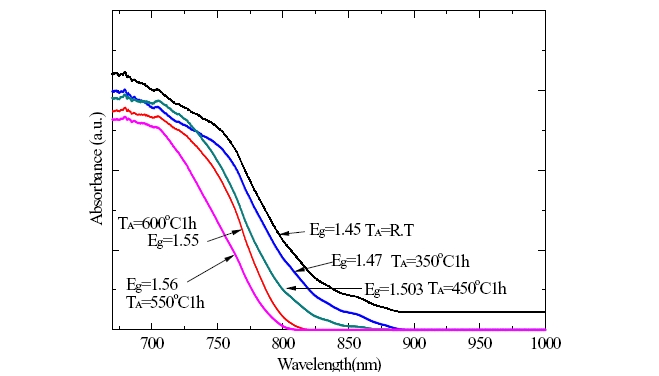
The optical absorption spectra of CuInS2 tin films with chalcopyrite structure at RT to 300℃ at intervals of 100℃ and the annealing temperature of thin film was varied RT to 550℃ in intervals of 100℃ were shown in Fig. 6.
The fundamental absorption wavelength, absorbance, and the energy band gap of p-type CuInS2 thin film with room temperature to 200℃ and an annealing temperature of 450℃ was 828 nm, 2×10⁻⁴ cm-1, and 1.503 eV, respectively. The energy band gap of p-type CuInS2 was 1.45 eV and 1.56 eV at an annealing temperature of RT to 550℃ respectively.
We know that the increased annealing with the sulfurization process was fundamental absorption moved onto the shorter wavelength, and the absorption coefficient decreased.
In this case, we concluded that a decrease in the reactive defect density made the grain size smaller and the last energy band gap larger.
The CuInS2 thin film was manufactured using sputtering and evaporation methods, and the annealing with sulfurization process was used in the vacuum chamber to vary the substrate temperature on the glass substrate, the annealing temperature and the composition ratio, and the characteristics thereof were investigated. As a result, the following conclusions could be drawn: (1) process conditions, which enabled the CuInS2 thin film having the desired composition ratio to be acquired by controlling each depositing rate of Cu, In and S, was established; (2) in the CuInS2 thin film, phase transition took place in the vicinity of 350℃ to 1h, and a thin film of a single phase was acquired at an annealing temperature of 450℃ to 1 hour; (3) the annealing with sulfurization process was used in the Vacuum chamber of S ambient carrier concentration, the Hall mobility and the resistivity of the p-type CuInS2 thin film as obtained through the experiment were 7.096×1017 cm-3, 53 cm2/V and 1.65×10⁻² Ω.cm, respectively. Also, optical energy band gaps of the films in S ambient appeared a little larger than those in the vacuum only.
The largest optical energy band gap of CuInS2 thin film in the Vacuum Chamber of S ambient was 1.503 eV. In light of the above results, it is thought that the CuInS2 thin film as obtained in this experiment has suitable physical properties to embody solar cells.