The AlGaN/GaN heterostructure exhibits advantageous materials properties such as wide band gap, superior carrier saturation velocity, thermal conductivity, and high breakdown field, which are required for high electron mobility transistor (HEMT). The AlGaN/GaN devices already show excellent performance in cell phone base stations and are promising candidates for power switching applications [1-6]. Most research concerning HEMTs has focused on improving power output and power added efficiency. Improvements in materials design and process control make these devices the most commercially accepted.
Excellent performance of GaN devices can be obtained routinely. However, relatively large gate leakage current, which can degrade power efficiency and noise performance, in GaN based devices is one of many undesirable characteristics. Growth defects and the mesa edge that are in contact with gate metal have been regarded as leakage current sources [7-10]. Photoluminescent emission is a useful technique in detecting photonic radiation from defect sites, primarily due to carrier recombination mechanisms. During device operation, defect sites emit light, which can be used identifying their locations.
Achieving acceptable device reliability and stability under continuous high performance operations is still required before commercialization. While several researchers have reported stable operation lives of more than 105 hours, these results are limited by relatively low frequencies and drain biases [5]. Reliability under high drain bias and high frequency conditions should be ensured before use in applications of high performance devices is considered. Although several mechanisms related to electrical degradation have been proposed, no clear explanation in terms of physical changes has yet been suggested.
In this study, in order to find the origin of gate leakage current, site specific transmission electron microscopy (TEM) analysis, in conjunction with photoemission microscopy (PEM) were used. We also report physical changes, using TEM and electron tomography, in AlGaN/GaN HEMTs after reliability tests. These results elucidate the correlation between device microstructure and its electrical properties.
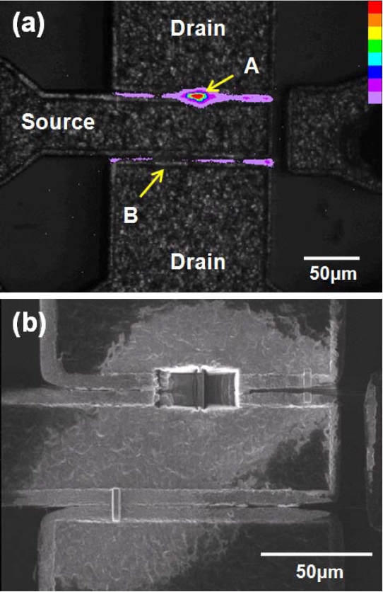
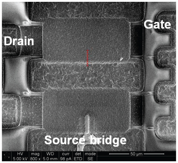
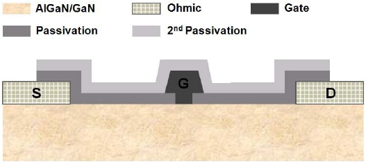
The AlGaN/GaN heterostructure is epitaxially grown on a SiC substrate via metal organic chemical vapor deposition (MOCVD). The device structure consists of 3 nm GaN cap/16 nm Al0.28Ga0.72N/2 μm GaN buffer layer/1 nm AlN barrier. A Pt/ Au metal gate 0.25 μm in length was deposited via evaporation. Standard III-V commercial production processing technology of TriQuint Semiconductor Inc. was used to fabricate the devices. SiNx passivation was used to connect the source pads. Overall structure is illustrated in Fig. 1. Standard structure of the device consists of four gate fingers with an air bridge connecting the sources (as shown in Fig. 4). Two-gated device without the air bridge was additionally fabricated for PEM tests in order to detect the emission from the gate (Fig. 2).
Photons with the infrared wave range of 1 to 3 μm were detected in PEM under bias conditions of VDS = 10 V, VGS = -5 V. The infrared images obtained via CCD camera were then overlaid with its corresponding optical images. Cross sectional TEM samples were prepared via the lift-out technique using a focused ion beam (FIB, FEI Nova200; FEI, Hillsboro, OR, USA) at positions corresponding to remarkable emission spots in PEM results. Bright field (BF) and high resolution TEM images were obtained with JEOL 2100F (JEOL Ltd., Tokyo, Japan).
For the accelerated DC life-tests, multi finger HEMT devices were subjected to stress under base-plate temperatures of 82, 112, and 142℃. A drain bias of 40 V and a time-zero drain current of 250 mA/mm were applied for 1,000 hours. Variations of drain current (IDQ) and gate current (IGQ) with time was recorded during tests. Device failure was defined as a drop in IDmax of more than 10%. Cross sectional TEM samples, all from the center of gate fingers, were prepared from over 80 failed devices. To obtain more detailed data on defect morphology, three-dimensional electron tomography was applied by acquiring TEM images every one degree in tilt angle in a range from -70o to 70o.
3.1 Defect for leakage current
In devices manufactured via standard processes, few devices showed high gate leakage current which is not in the acceptable range. In order to find the origin of the high leakage current, site specific PEM and TEM analyses were conducted. Fig. 2(a) is a PEM image obtained from the device exhibiting high leakage current. Light emission mainly occurs at the gate in the drain side. The luminescence along the drain side can be explained by a potential drop at the gate edge due to a change in potential distribution between the gate and drain electrodes [8]. A strong localized emission was observed at spot A in the upper gate finger while a very weak or no emission was detected at spot B. The emission irregularities indicate that the distribution of the electric field is not uniform along the gate.
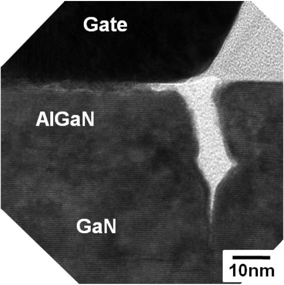
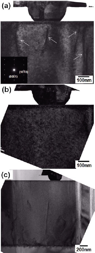
In order to discover the source of localized emissions, cross sectional TEM samples were prepared at spots A and B using FIB, as shown in Fig. 2(b). BF TEM imaging was conducted along the <10-10>; crystal direction of GaN. Mixed type of dislocations with edge and screw components in the AlGaN/GaN layer were detected below the gate in the sample from spot A, as indicated by arrows in Fig. 3(a). However, no dislocations were detected near the gate area in the sample from spot B, but dislocations were observed in the GaN layer near the interface with substrate (Figs. 3(b) and (c)). After several measurements, we found that the spots exhibiting high photon emission levels always have dislocations below the gate area. Based on site specific TEM observation in conjunction with PEM, the dislocations near the channel area, especially below the gate, are the source of gate current leakage, which results in photon emission irregularity along the gate.
Due to the 4% lattice mismatch between GaN and SiC substrate, high threading dislocation density is present in epitaxially grown GaN films, 107-1010 cm-2 [11,12]. These highly conductive dislocations are known to provide high leakage current pathway at room temperature [9]. Although the total density of threading dislocation has been reduced to within the range for acceptable device performance via improved processing technology, dislocation density is still higher than that of the other III-V compounds such as GaAs.
According to Bouya et al. [13], the observed emission irregularity is due to surface defects between SiN passivation and semiconducting layers. They observed delamination of SiN layer in the gate-drain space using cross sectional SEM observations after FIB milling. Non uniform distribution of the electric field, due to surface defects, was identified as the cause of emission irregularity. However, in our study, delamination of the passivation layer was not detected during FIB sectioning and TEM observation, indicating that the delamination is not the origin of gate leakage current in our case.
3.2 Physical degradation after reliability test
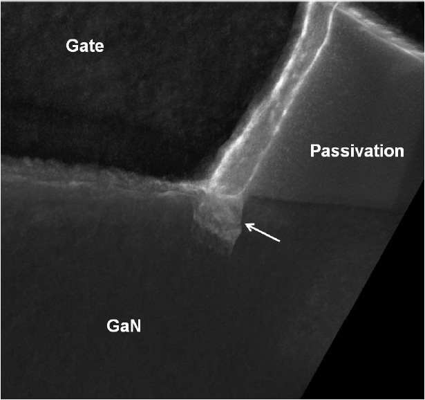
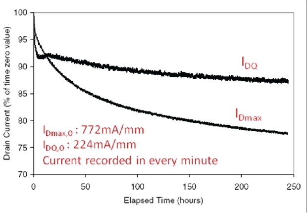
For the reliability test, four fingers packaged HEMTs with a configuration of 400 μm total gate length and source air bridge were used as shown in Fig. 4. Fig. 5 shows the typical degradation of electrical properties during the tests. The decrease in IDmax was used as a barometer to delineate the degree of electrical degradation. TEM analyses were conducted at the middle of the center gate finger since the area has the geometrically lowest cooling efficiency, resulting in the highest joule heating temperature. The results revealed that electrically degraded devices always contain a pit/crack shaped defect at the gate edge in the top AlGaN layer, as shown in Fig. 6. A vertical crack propagates through the interface between AlGaN and GaN layer. Degradation of the AlGaN crystal structure just below the gate is indicative of the damage to the AlGaN channel layer. In the cases where devices showed minimal degradation, a shallow pit is observed only in the drain side. In contrast, severely degraded devices always have a large pit/crack in the drain side. Previously we reported a strong correlation between the degree of physical damage and the drain current (IDmax) degradation in terms of 'disfiguration factor' [14]. The concentration of temperature increase, strain development, and carrier traps on the drain side [15-17] is an indication of drain side, gate edge defect formation.
A drawback of TEM analysis is that the two dimensional image may lead to an incorrect interpretation of overall sample geometry. Thus, the application of the three dimensional tomography provides more accurate and detailed information about defects observed in TEM images. TEM images acquired in every one degree in tilt angle from -70° to 70° were reconstructed into a single three dimensional feature. Figure 7 is a snapshot from the reconstructed video showing the three-dimensional morphology of the defect displayed in Fig. 6. The crack that has formed in the channel extends for the entire thickness of the TEM lamella, as indicated by the arrow. The crack detected at the center of the gate finger was also observed in multiple sections along the gate finger, indicating that physical features of a sample are representative of the physical features of the whole device [18]. Furthermore, tomography shows a more unclear interface between the channel and gate metal than that between the AlGaN and passivation layer. Surface defects of channels are found only in devices with severe electrical property degradation.
Several mechanisms for HEMT device degradation during operation have been suggested. However, there is no mechanism that sufficiently explains all the observed physical damage. It is known that AlGaN layer grown on GaN has a tensile in-plane misfit strain [19]. The tensile strain may account for the greater crack width in the AlGaN layer than that of the GaN layer. In addition, applied voltage in the AlGaN/GaN HEMTs causes the greatest amount of inverse piezoelectric strain/stress near the gate edge on the device [17]. Based on our observations, we believe that accumulated in-plane stress, a combination of the misfit strain and the inverse piezoelectric effect in the channel, is responsible for physical degradation of HEMT devices. However, this mechanism cannot sufficiently account for the formation of round pits in minimally degraded devices.
Device lifetimes showed significant sample to sample variation. Even devices fabricated by identical processes on the same wafer showed extremely high variation in lifetimes [18]. Also, as described earlier, the irregular leakage current was observed by PEM. Threading dislocations in the channel area below the gate are suspected to be the main pathways for gate leakage current. Leakage current and degradation during operation are believed to be related with stress/strain developed in channel layer. However, we could not, as of yet, find a direct correlation between these phenomena. The irregular leakage current and lifetime in GaN HEMT devices need to be further investigated to improve their performance and reliability.
The origin of gate leakage current and electrical properties degradation during life test in production quality AlGaN/GaN HEMT devices were investigated by various microscopy techniques. Irregular light emission along the gate was detected in the devices by PEM, indicating high leakage current. Site specific TEM analyses revealed that threading dislocations in the channel area below the gate, resulting from lattice mismatch with the substrates, act as high leakage current pathways. After reliability tests of devices under a high drain bias of 40 V, physical defects, such as pits and cracks, under the drain next to the gate, were observed in the electrically degraded devices. There is a strong correlation between the degree of physical damage and the degradation of electrical properties. Leakage current and reliability of HEMTs involve mechanical stress in the channel area.