Transparent conducting oxide (TCO) films have been widely used for mobile display applications, such as organic lighting diodes, liquid crystal displays (LCD), micro displays, and solar cells [1]. Until now, indium tin oxide (ITO) films have been popular amongst TCO materials because of high stability and low resistivity. However, ITO meets the requirements of transparent conducting thin films which has made it a commodity and is in short supply, as indium is somewhat rare and expensive [2].
Recently, zinc oxide (ZnO) has been considered an ideal alternative material due to its lower cost and wide availability [3], [4]. Recent research reveals that Al?, B?, Ga?, and Mndoped ZnO films show low resistivity and high transmittance [5]?[8]. Also, to obtain high?quality ZnO films, a variety of techniques may be used, such as RF magnetron sputtering, pulse laser deposition (PLD), sol?gel, and DC sputtering [9]?[12]. A radio frequency (RF) magnetron sputtering method is generally used for TCO film synthesis. For some product applications, the TCO must be synthesized at lower temperatures, such as under 200℃ [13].
In this study, we investigated the effects of RF power on the structural, electrical, and optical properties of Al?doped ZnO (AZO) films. We used an AZO target (Al: 2 wt.%) to synthesis AZO films, which were deposited at room temperature. The thickness of all the films was kept constant at 150 nm, because this is the thickness of TCO electrodes used in LCD products.
The AZO films were deposited on a glass (OA?10G; Nippon Electronic Glass Co., Ltd., Tokyo, Japan) substrate by an RF magnetron sputtering system. Before the operating plasma, the substrates were cleaned with trichloroethylene, acetone, methanol, and distilled water (D.I. water), for 10 minutes respectively. The sputtering chamber was pumped down to 5 × 10?6 torr by a turbo molecular pump. Highly pure (99.999%) argon was applied as the sputtering gas, and the AZO (Al: 2 wt.%) target had a diameter of 4 inches. Pre?sputtering treatment was performed to clean the target surface for 10 minutes by argon plasma. A distance of 6 cm was kept between the target and substrate. Furthermore, the substrate was rotated at 1,700 rpm. We changed the deposition RF power from 100 W to 350 W in steps of 50 W, while the other conditions were fixed. The thickness of all films was kept constant at 150 nm, so deposition time varied with the RF power.
The thickness and cross?sectional images of the films were checked by field emission scanning electron microscopy (FESEM; S?4800; Hitachi, Tokyo, Japan), and the crystallinity of the AZO film was analyzed with X?ray diffraction (XRD; Max 2500H; Rigaku, Tokyo, Japan). The electrical properties were investigated using a Hall measurement (HMS?3000; Ecopia, Arizona, USA) and a four?point probe (CMT?SR2000N; AIT, Suwon, Korea). The transmittance of the AZO films was investigated using an ultraviolet/visible (UV/VIS) spectrometer (S?3100; Scinco, Seoul, Korea).
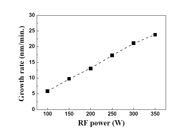
Figure 1 shows the growth rate of the AZO films as a function of RF power. The growth rate increased linearly as RF power increased. Based on this result, we fixed the film's
thickness to 150 nm by adjusting the deposition time.
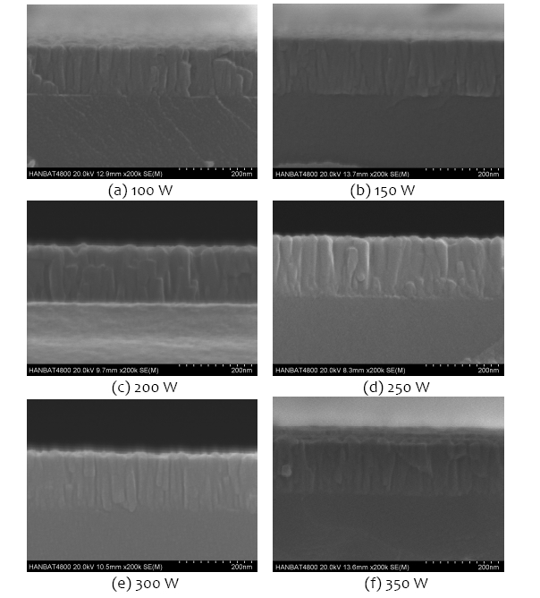
Figure 2 shows the cross?sectional SEM images of the AZO films as a function of RF power. The thicknesses of the films were 150 nm. We confirmed that all films were grown as columnar structures, oriented around the c?axis.
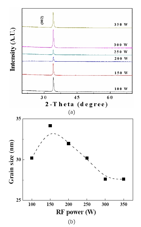
Figure 3 shows the XRD patterns of the AZO films deposited on the glass substrate. Fig. 3(a) shows that all AZO films had highly preferred orientation (002) peaks. The intensities of the (002) direction of the main peaks decreased according to an increase of the RF powers from 100 W to 250 W. However, in case of 300 W and 350 W of RF power, the intensities increased, and other (004) peaks were also observed. According to Scherrer’s equation [14], the grain size could be calculated with the full width at half maximum (FWHM) value. The FWHM values of 100 W and 150 W were decreased from 0.31 to 0.26, but the values between 200 W and 350 W increased from 0.28 to 0.35. Fig. 3(b) shows the grain size of the AZO films as a function of the RF power calculated by Scherrer’s equation. The grain sizes varied from 27.6 nm to 34.2 nm in the range of 100 W to 350 W RF power. We obtained the highest value of 34.2 nm at 150 W RF power.
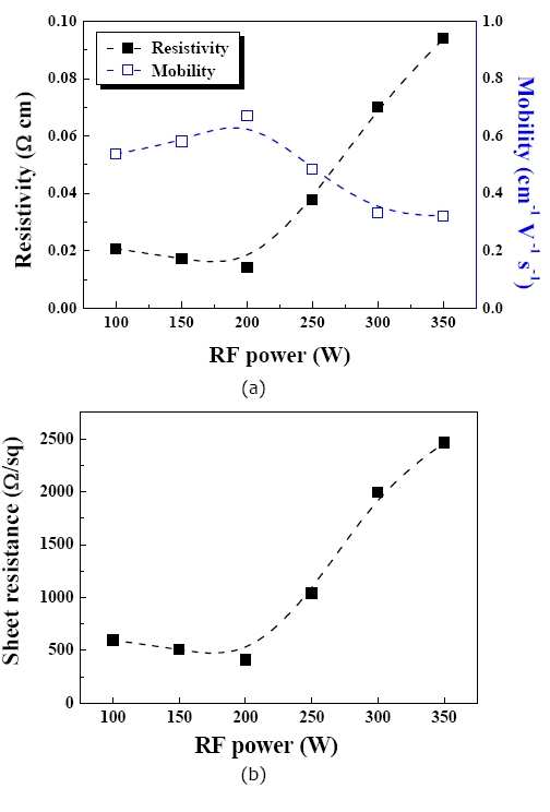
Figure 4(a) shows the dependence of electrical resistivity and mobility as a function of RF power. The resistivity of the AZO films decreased when the RF power was increased from 100 W to 200 W and showed the lowest resistivity (0.014 Ω?cm) at an RF power of 200 W. However, the resistivity of the AZO films increased as the RF power increased from 250 W to 350 W. On the contrary, Hall mobility increased from
0.54 cm?1V?1s?1 to 0.67 cm-1V?1s?1 at the RF powers of 100 W to 200 W. Fig. 4(b) shows the four?point probe results as a function of RF power. The sheet resistance of the AZO films decreased as the RF power increased from 100 W to 200 W and showed the lowest sheet resistance (411 Ω?sq) at an RF power of 200 W. However, the resistivity of the AZO films increased as the RF power increased from 250 W to 350 W. This result was entirely consistent with the Hall measurement results. As confirmed by XRD results, the crystallinity of the AZO films grown at room temperature was sensitive to the deposition RF power which indicated that the resistivity of the AZO films was influenced by the crystallinity.
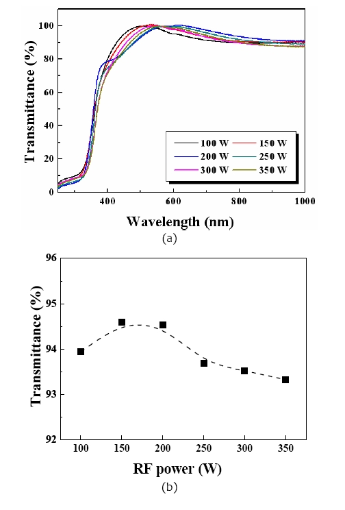
Figure 5(a) shows transmittance spectra of AZO films measured by a UV?VIS spectrometer, and the average (400? 800 nm) transmittances are summarized in Fig. 5(b). The transmittance of the AZO films increased as the RF power increased from 100 W to 200 W and showed the highest resistivity (94.59%) at the RF power of 150 W. However, the transmittance of the AZO films decreased as the RF power increased from 250 W to 350 W. All of the AZO films showed a high transmittance of over 90%. The average transmittance was slightly changed by the RF power.
The AZO films were deposited on glass substrates by the RF magnetron sputtering method using an AZO target (Al: 2 wt.%) at room temperature. We investigated the effect of RF power on structural, electrical, and optical properties of 150? nm?thick AZO films. XRD results showed that AZO films have highly preferred orientation (002) peaks. The grain size of the AZO film in the cases of 150 W and 200 W RF power were 27.6 and 34.2 nm, respectively. Also, RF powers of 150 W and 200 W provided good electrical and optical properties. The resulting values for 150 W and 200 W are summarized as a resistivity of 0.017 Ω?cm and 0.014 Ω?cm, a sheet resistance of 510 Ω?sq and 411 Ω?sq, and a transmittance 94.59% and 94.53%, respectively.