The design of high efficiency direct current (DC)?DC buck converters becomes important since battery operated portable electronic devices are in great demand. A current?mode buck converter is usually composed of a feedback network, a switching element, and an output filter [1], [2]. The feedback network is an on?chip integrated circuit that performs a current? mode pulse width modulation (PWM) control. By using the properties of bipolar transistor, a high performance PWM circuit can be manufactured. It enables an accurate sensing of an inductor current that has a high frequency and currentdriving capability.
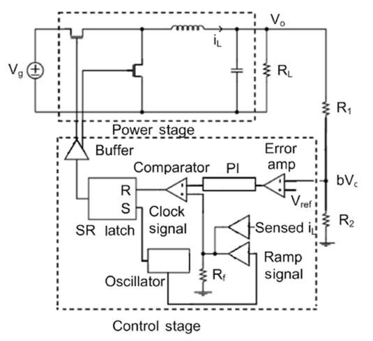
Figure 1 shows the structure of a current?mode buck converter with an off?chip LC filter. The converter is composed of a power stage and a feedback network. In order to provide a low power and fully integrated power module, a monolithic current?mode DC?DC buck converter with an on?chip current sensor used for feedback control has been designed using the standard 0.35 ㎛ complementary metal?oxidesemiconductor (CMOS) process. The converter is implemented with a synchronous rectifier in such a way that the forward?bias diode voltage drop is eliminated. The power switches, the feedback circuit, and the current?sensing circuit are designed to be on?chip. An off?chip inductor and capacitor are required for the low pass filter; thus reducing the number of I/O pins and the number of reactive components needed for the converter. The off?chip LC filter is designed with an inductance of 1 mH and a capacitance of 12.5 nF. The output voltage is scaled down by R1 and R2. It is compared with the reference voltage before being fed into the error amplifier. The output of the error amplifier, the compensation ramp, and the sensed inductor current signal will pass through the comparator and the S?R latch in order to define the duty cycle ratio. The duty cycle ratio controls the switching times of the power transistors in such a way that a negative feedback is created to regulate the output voltage. Although current?mode control is much better than voltagemode control, there are a lot of difficulties and problems for circuit realization of the current?sensing function [3], [4]. Many current sensing approaches have been proposed. However, poor current?sensing accuracy, efficiency degradation, and complicated circuit implementation are problems
that occur in effective IC design. Therefore, the sense metaloxide? semiconductor field?effect transistor (MOSFET) method used for current sensing is proposed for a low?voltage current?mode buck converter.
Another method that is able to provide solutions to many problems of the existing current?sensing schemes is the application of bipolar CMOS (BiCMOS) technology. Compared to regular MOS devices, bipolar devices exhibit superior conductance and low noise. These attributes allow bipolar circuits to apply low noise amplification over large bandwidths. On the other hand, CMOS circuits provide the advantage of high speed and low power consumption. BiCMOS technology usually combines bipolar and CMOS circuits onto one IC chip [5], [6]. Through the selective use of these advantages, BiCMOS technology can offer the possibility of a high performance in power electronic circuits.
In this work, a current?mode buck DC?DC converter with bipolar and CMOS circuits is presented with the sense MOSFET method used for the current sensing. The DC?DC converter is designed using the standard 0.35 ㎛ CMOS process. The proposed circuit is tested by the post layout simulation and expected to show a much better performance as compared to the conventional CMOS circuit.
Current sensing is the one of the most important functions in a current?mode DC?DC converter. Most DC?DC converter sense the inductor current for over?current (over?load) protection, regardless of the type of feedback control. Additionally, the sensed current is used in the converter for loop control. Since the instantaneous changes in the input voltage are immediately reflected in the inductor current, current?mode control can be used to determine when to switch between the continuous?conduction mode (CCM) and the discontinuous? conduction mode (DCM), which results in an overall increase of the efficiency of the DC?DC converter. The sense MOSFET (SENSEFET) method is the practical technique for current sensing in power MOSFET applications [7]?[9]. The technique is to build a current sensing FET in parallel with the power MOSFET. The effective width of the SENSEFET is sig?
nificantly smaller than the power FET. The width of the power MOSFET should be at least 100 times the width of the SENSEFET in order to guarantee that the power consumption in the SENSEFET is low and quasi?lossless. The voltages at the sources of the SENSEFET and the power FET should be equal to eliminate the current mirror non?ideality that results from channel length modulation. An op?amp is used to force the voltages at the sources to be equal. As the width ratio of the main MOSFET and the SENSEFET increases, the matching accuracy of the FETs degrades. The bandwidth of this technique is reported to be unexpectedly low and can not be estimated by RC pole analysis. Since the current ratio in the SENSEFET circuits is on the order of hundreds, even a low degree of coupling between the power MOSFET and the SENSEFET circuits can induce a significant error, and large spikes should be expected in the sense signal during periods of high di/dt. Therefore, a proper layout scheme should be considered to minimize the reactive components in the power MOSFET and the SENSEFET circuits.
BiCMOS technology combines bipolar and CMOS circuits onto one IC chip. The aim is to combine the low power, the high input impedance, and the wide noise margins of CMOS with the high current?driving capability of bipolar transistors. CMOS, although a nearly ideal logic?circuit technology in many respects, has a limited current?driving capability. This is not serious problem when the CMOS gate has to drive a few other CMOS gates. On the other hand, a bipolar junction transistor (BJT) is capable of large output currents by virtue of its large transconductance. A practical illustration of that is in the emitter?follower output stage of an emitter coupled logic (ECL). The high current?driving capability contributes in making the ECL much faster than CMOS at the expense of high power consumption. Since the BiCMOS technology is well suited for the implementation of high?performance analog circuits, it makes possible the realization of both analog and digital functions on the same IC chip. The current sensor is designed with a matched pnp transistor with the power pchannel MOS transistor. The error amplifier and the currentsensing circuit are designed with BiCMOS technology in order to achieve a low power consumption and a high input impedance with the high current?driving capabilities of a BJT.
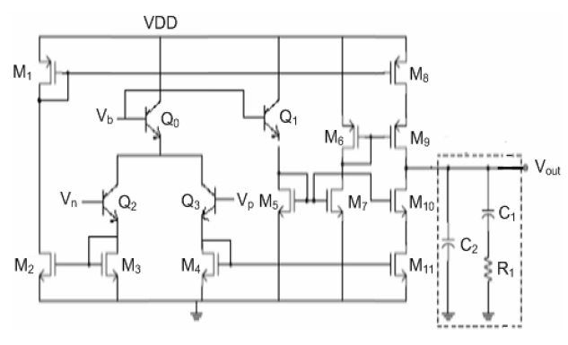
The circuit implementation of the error amplifier is shown in
Fig. 2, which is mostly composed of a cascode operational transconductance amplifier (OTA) and a compensator. The cascode OTA is used in this converter as it is a single?stage amplifier that has a high gain and only one dominant pole. In order to fully exploit the advantages offered by BiCMOS technology, the differential bipolar transistor pair Q2 and Q3 with a cascode bias forms the input stage for the error amplifier. The current required for the operation of the differential amplifier is provided by current mirrors and the cascode bias. Most of the MOS transistors shown in the circuit are used for the current mirror.
For the power stage of the current?mode converters, the control?to?output transfer function has two separated poles. The pole from the output filtering capacitor is dependent on the output load resistor. A compensator in the feedback network is used to generate the pole and the zero used for the pole?zero cancellation. The control?to?output function will yield a sufficient phase margin below the unity gain frequency. The unity gain frequency should not be too close to the converter’s switching frequency as the amplifier would then amplify the output ripple voltage. A sufficient margin for the unity gain frequency should be below 20% of the switching frequency.
2.2 The current?sensing circuit
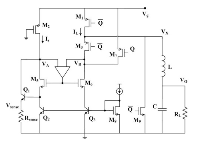
The current sensor is designed to use the power PMOS transistor M1 and the SENSEFET M2. The matching of transistors M1 and M2 depends on the process parameters such as the mobility μ, the oxide capacitance Cox and the threshold voltage VT. An op?amp is used as a voltage mirror to enforce the same voltage at voltage VA and voltage VB. Any change in VA will force a similar change in VB due to the virtual shortcircuit provided by the op?amp. Thus the drain?source voltage VDS of transistor M2 is almost same as the drain?source voltage VDS of transistor M1. However, transistors M1 and M2 are scaled so that the power transistor M1.on the output side of the circuit, has an aspect ratio of 100:1 which is much greater than that of transistor M2, located on the sensing side. As a result, the Is current on the sensing side is much smaller than the Io current on the output side.
The output sensing current Isense, which passes through the resistor Rsense, is the difference between the sensing current
IS flowing through the transistor M2 and the current I2 flowing through the small biasing current source. For a small biasing current I2 ≪ IS, the current Isence flowing through Rsense is almost proportional to the current flowing through the inductor and much smaller than the inductor current. For the current mode DC?DC buck converter application, only the sensing? voltage Vsense is needed in the control feedback loop during the on?state; the signal from the power transistor M1 during the turn?on is sensed. Thus, the design of the amplifier is also very important in this sensing circuit as it will affect the minimum supply voltage, the accuracy of the sensing voltage and the stability of the whole sensing circuitry.
As the sensed inductor current is scaled down, the power loss in the sensing circuit is significantly reduced. The accuracy of the sensed inductor current depends on the current mirror of transistors M1 and M2, seen in Fig. 3, and the resistor Rsense, as stated in the equation, respectively. An op?amp is used as a voltage mirror in such a way that the sensing current Isense is matched to the inductor current IL. The sensing signal Vsense is given by:
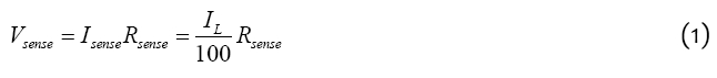
The resistor Rsense is used to convert the current signal to a voltage signal in such a way that Vsense is proportional to the sensing current. Since the op?amp is used to enforce voltage VA to be the same as voltage VB, a high gain amplifier is needed for an accurate current?sensing. This kind of currentsensing circuit still has some undesirable problems, such as the offset?current, the accuracy, and the sensing speed because the sensed current is the sum of the scaled inductor current and the biased offset?current. The simulation results show that the delay time is less than 5 ps, which can be adjustable for an application with the switching frequency of less than 200 MHz.
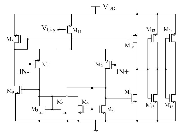
The comparator used for the PWM control, shown in Fig. 4, is implemented using a cascaded bias, a source?coupled differential pair, and inverter chains. The source?coupled differential pair with positive feedback is used to provide a high gain; the inverter chains M12?M15 are used to obtain a clear logic response. The inverter chains can also act as a driver
stage so transistors M7 and M8 can be made smaller in order to reduce the parasitic capacitance resulting in a faster response.
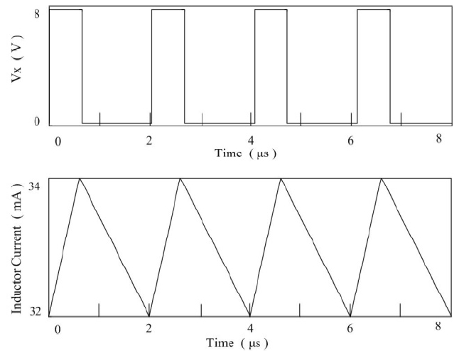
Figure 5 shows the sensing voltage Vx and the inductor current at an input voltage of 8 V with a 0.3 duty ratio. The inductor current is sensed and scaled to Isen. The Isen is then added to the pulse?width modulation controller, which is formed by a voltage comparator, an SR latch, and an oscillator to generate the signal used to control the duty cycle. The sensing voltage indicates the exact input voltage of 8 V and the duty ratio of 0.3 after passing the feedback circuit. The slope of the inductor current provides the feedback output voltage and inductance information. The average inductor current is about 33 mA. The discharge time is about 1.3 μs. The proposed current?sensing circuit is seen to sense the charging of the LC filter accurately. The error between the sensing signal and the inductor current is within 3%.
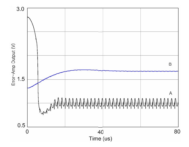
The error amplification is tested by comparing the circuit which replaces the bipolar transistor with the MOSFET. The amplification characteristics shown in Fig. 6 indicate a higher output voltage with a smaller ripple in the proposed circuit, which indicates much better characteristics in the error amplifier which utilizes BiCMOS circuits. The BJT is capable of large output currents by virtue of its much larger transconductance. In the error amplifier circuit shown in Fig. 2, BJTs are used for the difference amplifier and the current source, thus providing a larger voltage gain and output resistance than is possible with a conventional MOS circuit.
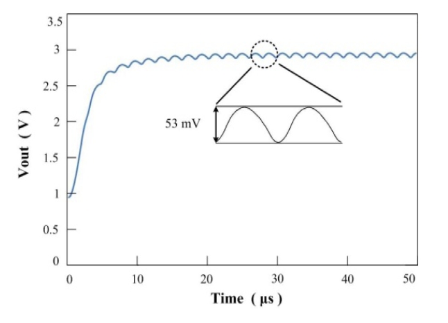
Figure 7 represents the waveforms of the output signal and ripple voltage at an input voltage of 8 V. It is obtained at a duty cycle of 30%, an inductance of 1 mH, and a capacitance of 12.5 nF. The ripple voltage can be significantly reduced with an increase of the inductance or the capacitance in the off?chip low pass filter. The expected output and ripple voltages are obtained with this result; the ripple voltage is controlled within 3%. The switching frequency of 500 kHz is more than ten times higher than the characteristic frequency of the
LC filter, so the converter operates in the continuousconduction mode and the ripple is independent of the output load power.
A current?mode DC?DC converter was designed using the 0.35 ㎛ CMOS process with single?poly and four?metal at the switching frequency of 500 KHz. The converter is largely composed of a power stage and a feedback network. To obtain a high performance converter, the SENSEFET method and BiCMOS technology are applied in the current?sensing circuit. In the error amplifier, a cascode OTA and BiCMOS technology are used to achieve a high gain and uses only one dominant pole. The simulation test shows that the error between the sensing signal and the inductor current is within 3% and the output voltage ripple is controlled within 3% at a power efficiency of 85%. The result indicates that the currentmode DC?DC converter using the SENSEFET method and BiCMOS technology shows good performance in terms of current sensing, ripple voltage, and power efficiency.