Transparent conducting oxide (TCO) thin films have been extensively studied because of their high optical transparency and electrical conductivity. They are used in photo electronic devices such as solar cells and flat panel displays. Of all the TCO films, indium tin oxide (ITO) is the most widely used anode material in flat panel displays such as liquid crystal display (LCD), plasma display panel (PDP) and OLED [1], [2]. ITO thin films have been extensively utilized in these devices because of their high transmittance in the visible range and low electrical resistivity. ITO films can be deposited by many kinds of deposition system such as pulsed laser deposition [3]-[5], chemical vapor deposition [6], and RF magnetron sputtering [6]-[8]. Amongst these methods, r.f. magnetron sputtering technique has been widely used due to its advantageous features including simple apparatus, high deposition rates, and low deposition temperature [9].
The properties of ITO thin films depend strongly on the stoichiometry, microstructure and the nature of the impurities and it is obvious that deposition processes associated with different control parameters induce slightly different characteristics in thin films. The effect of oxygen in the reactive sputtering on the electrical and structural properties of ITO films has been studied by several groups [10], [11]. The roles of the partial pressure of oxygen and hydrogen on the structural as well as the optical and electrical properties of r.f. magnetron sputtered ITO films were also discussed [12]. From these studies, it is concluded that the electrical resistivity correlates strongly with the stoichiometry of the ITO thin films.
Considering these facts, it is interesting to study the effect of the ambient gas on the structure and the electrical resistivity, and especially on the charge carrier concentration and charge mobility of the ITO thin films. Furthermore, in this study, we have investigated the effect of the structure and electrical resistivity of ITO thin films on the performance of OLED devices. For this purpose, Sn-doped In2O3 (ITO) films were deposited by r.f. magnetron sputtering under various ambient gases (Ar, Ar+O2, and Ar+H2). The electrical resistivity and the surface morphology of the TCO thin films were systematically examined. In order to elucidate the effect of the electrical resistivity on the performance of OLED devices, the organic materials and cathode electrode were sequentially deposited on the TCO thin films. Then, the electrical characteristics such as current density vs. voltage and luminescence vs. voltage of OLED devices were measured.
The ITO thin films were prepared by r.f. magnetron sputtering with a mixture of a 90% indium oxide and 10% tin oxide target. The glass substrates (corning 7059, SAMSUNG CORNING PRECISION GLASS, KOR) were first cleaned with standard cleaning procedures and then rinsed in deionized water. The sputtering chamber was evacuated by a turbomolecular pump to the base pressure of about 1.0×10⁻⁶ torr. In order to investigate the influences of
[Table 1.] Conditions of sputtering ITO thin films.
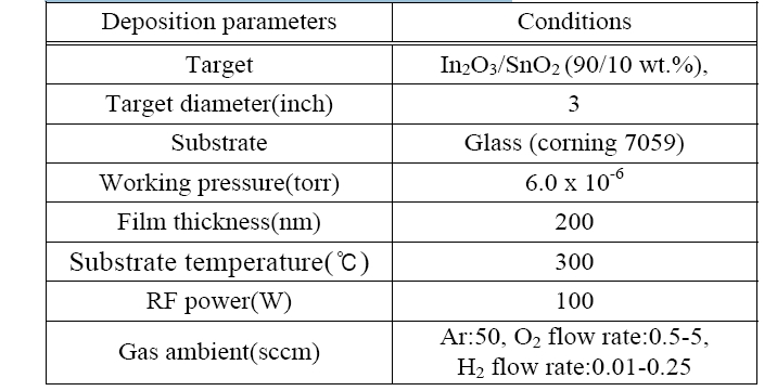
Conditions of sputtering ITO thin films.
the oxygen and hydrogen, the flow rate of oxygen and hydrogen in the argon mixing gas has been changed from 0.5 sccm to 5 sccm and from 0.01 sccm to 0.25 sccm, respectively. The sputtering gas was Ar and the substrate temperature was 300℃. Table 1 indicates the experimental conditions for the deposition of ITO films.
The microstructural observation and crystal orientation of the ITO thin films were evaluated by using X-ray diffraction and an FESEM (field emission scanning electron microscope), respectively. The optical transmittance of ITO thin films was measured using an ultraviolet spectrophotometer (model cary500, Varian, KOR). The film thickness was determined using a surface profile measurement system and the electrical properties of the ITO thin films were measured using hall effect measurement (model HMS-3000, ECOPIA, KOR). Then, the organic materials and cathode electrode were sequentially deposited on the TCO thin films. The device structure was TCO/α- NPD/DPVB/Alq3/LiF/Al. The DPVB was used as a blue emitting material. The electrical characteristics such as current density vs. voltage and luminescence vs. voltage of the OLED devices were evaluated by using a spectrometer (model CS- 1000A, KONICA MINOLTA SENSING INT, JPN).
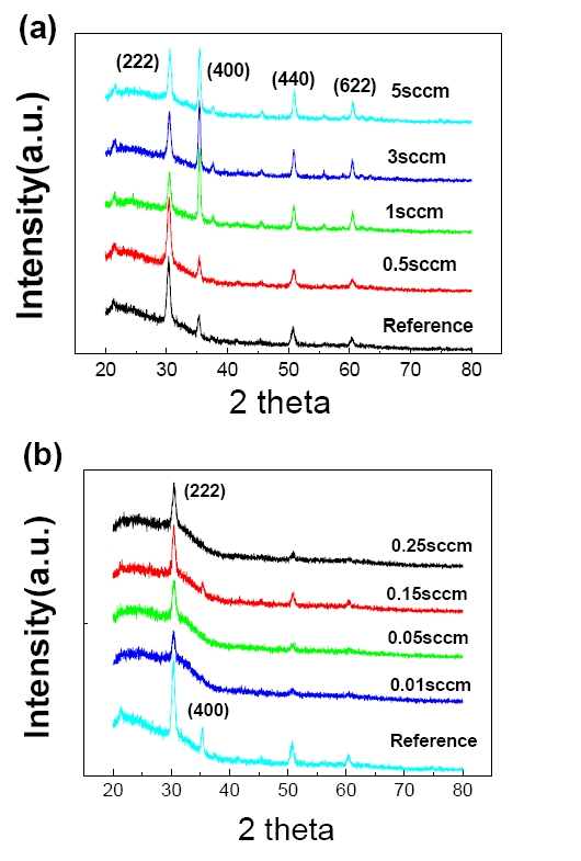
XRD patterns of the ITO thin films deposited using r.f. magnetron sputtering are presented in Fig. 1. The Figure clearly indicates that the ITO phase is fully stabilized (within a detection limit of XRD) and the crystal orientation is influenced considerably by the ambient gases. Here (222) and (400) are the most prominent peaks indicating that the ITO film has an (111) and (100) preferential orientation. Oxygen vacancies in the ITO thin films deposited under Ar ambient gas play important roles in atomic diffusion and oxygen atoms can diffuse through these vacancies. Therefore, various preferred planes are formed in argon sputtered ITO thin films [13]. It is very interesting to note in Fig. 1(a) that with the increase of oxygen concentration, the (222) major peak remains unaltered and the peaks at (400), (440), and (622) are dominant. Figure 2(b) shows that the (222) major peak remain unaltered and the peaks at (400), (440), and (622) are nearly invisible in the Ar+H2 atmosphere. It has been reported that a specific preferred orientation of thin film can be discussed on the basis of
strain and surface energies. At small film thicknesses the surface energy controls growth and at large film thicknesses the strain energy predominates. Based on the above discussions, we can conclude that the (400) plane of ITO thin films has the lowest strain energy and is directly associated with the atomic diffusion of oxygen.
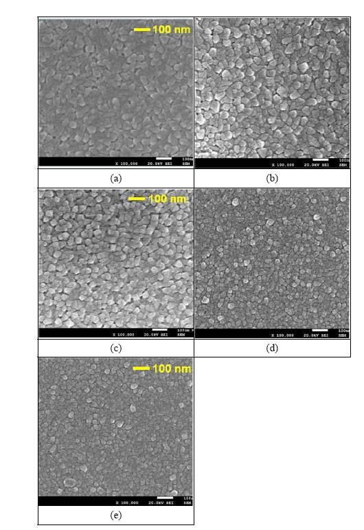
Microstructural features of the ITO thin films with different ambient gases are presented in Fig. 2. As shown in the figures, the second phases are not observed. The grain sizes in ITO thin films deposited under Ar and Ar + O2 ambients are nearly the same and small voids are observed in between the grains regardless of O2 flow rate. However, for the films deposited under Ar+H2, the average grain size decreases and voids in the grain boundary region are much less. From the results of Figs. 1 and 2, it seems that the ambient gases have an important effect upon physical characteristics such as crystal orientation and the microstructure of thin films.
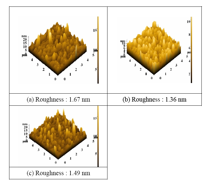
Since the surface properties of the ITO thin films may affect the characteristics of the OLED devices [14], it is very important to investigate the surface morphology of the ITO
thin films. Figure 3 presents the AFM images of ITO thin films deposited under the various ambient gases. As shown in the figures, all surfaces are very flat and no very sharp peak appears in the domain. Furthermore, it seems that the surface roughness is not directly related to the concentration and kind of ambient gas.
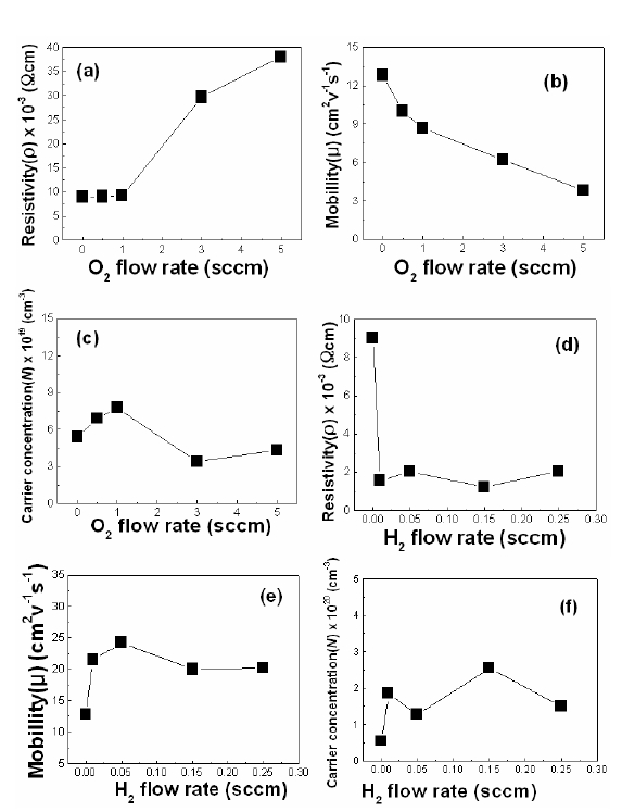
Figure 4 presents electrical resistivity (ρ), charge mobility (μ), and charge carrier concentration (
increases. Under reactive sputtering with hydrogen, due to the reducing property of hydrogen, oxygen vacancies are created in ITO thin films. Therefore, the resistivity of such films, deposited under Ar + H2 gas ambient is much lower compared to that of the film deposited under Ar + O2. Contrary to this discussion, from the results of Fig. 4, it is
important to note that the electrical resistivity of ITO thin films is mainly associated with the charge carrier mobility rather than the charge carrier concentration. Furthermore, from the results of Fig. 1 and Fig. 4, the behavior of the electrical resistivity and the charge mobility is nearly similar to that of the peak intensity of the (400) orientation of ITO thin films. This observation suggests that the structure of ITO thin films associated with oxygen atoms and oxygen vacancies is related with the electrical properties,, especially charge mobility. A more systematic and concrete analysis will be worthwhile, and this will be reported in a following paper.
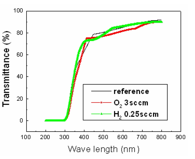
Figure 5 presents the optical property of the ITO films with different ambient gases. The figure shows that the average transmittance in the visible wavelength region is over 80% for all the ITO thin films. The ITO film deposited under ambient Ar + H2 shows a higher transmittance compared to that deposited under Ar and Ar + O2, which can be explained in terms of the more compact and void free microstructure of the ITO thin films (Fig. 2). The increase in transmittance over a wider wavelength range may be beneficial for certain applications of TCO thin films, e.g. as a window layer in thin film solar cells.
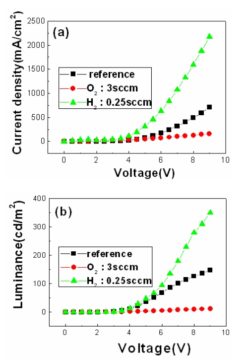
Figure 6 shows (a) the current density vs. voltage and (b) the luminance vs. voltage characteristics of the OLED devices with the ITO thin film deposited in various ambient gases for comparison. The device structure is TCO/α- NPD/DPVB/Alq3/LiF/Al. The DPVB is used as a blue emitting material. As shown in Fig. 6(a), the current density of OLED devices with ITO thin films deposited in Ar+H2 ambient gas rises more sharply than that of ITO thin films deposited in O2 ambient gas. This implies that the ITO anode deposited in Ar+H2 ambient gas has higher hole injecting ability than that of ITO thin films deposited in O2 ambient gas. As shown in Fig. 6(b), the luminance of OLED devices with ITO thin films deposited in Ar+H2 ambient gas is the highest amongst all other films considered. From the results of Figs. 6, one can clearly conclude that the electrical resistivity of ITO thin films plays a major role in OLED device performance, especially the current density and luminance.
The structural, electrical, and optical properties of the ITO thin films were systematically examined for use as the anode contact in OLED device and we obtained the following conclusions.
(1) ITO thin films were deposited by RF magnetron sputtering under the different ambient gases (Ar, Ar+O2, and Ar+H2) at 300℃.
(2) The relative intensity of (400) peak of ITO thin films is increased with increasing the flow rate of O2, while the (400) peak was nearly invisible in Ar+H2 atmosphere.
(3) The electrical resistivity of ITO thin films increases with increasing O2 flow rate, and dramatically decreases under Ar+H2 atmosphere. Furthermore, in the case of H2 atmosphere the electrical resistivity is nearly similar regardless of H2 flowing rate. It is important to note that the electrical resistivity of ITO thin films is mainly associated with the charge carrier mobility.
(4) All the films have a high transmittance regardless of ambient gases.
(5) The current density and luminance of OLED devices with ITO thin films deposited in Ar+H2 ambient gas is the highest amongst all the ITO thin films prepared under different conditions