A conventional discrete power chip consists of bipolar transistors, and has a high power-driving capability, but it has relatively low level of integration, and is not power efficient. By contrast, a complimentary metal-oxide semiconductor (CMOS) transistor consumes less power but has a low current-driving ability. Therefore, a bipolar transistor is suitable for implementing analog functions, and a CMOS transistor is used in low-power digital circuits. Recently, there has been a growing demand for power chips that use a new bipolar-CMOS-DMOS (BCDMOS) process that can significantly improve device performances and decrease chip size by putting both analog and digital functions onto a single chip in very-large-scale integration (VLSI) systems [1]-[3]. The chip contains both laterally diffused metal-oxide-semiconductor (LDMOS) devices (12 V) for driving power transistors and CMOS devices (3.3 / 5 V) for driving digital high-speed operations [4], [5]. Because the gate voltage levels of these two types of transistors are different, the chip will normally contain a level shifter that acts as a voltage buffer in order to achieve a high-speed data interface between the transistors [6]. However, in a low gate source voltage (Vgs) LDMOS device, the conventional 12 V gate voltage is reduced down to the 3.3 / 5 V level, which makes it possible to have a direct interface between the CMOS and the LDMOS without the use of a level shifting circuit, and this improves several aspects, namely the chip’s speed, its power efficiency, and the overall size-effectiveness without requiring a level shift circuit, as compared to the conventional 0.35 ㎛ BCD process. In addition, a low Vgs LDMOS element was embodied which is specific on resistance (Rsp) optimized by applying a double gate oxide.
In most cases the gate driver in a class D-audio amplifiers currently available in the displays market which is one of main applications using the 0.35 ㎛ BCDMOS process, all of high power elements greater than 20 W are generally of N-type for both of upper and lower sides because N-type is better than P-type with respect to switching speed and Rsp.
For gate voltage drain drain (GVDD) and VDD for supplying power to the gate driver and the analog circuits, 12 V is applied in the 0.35 ㎛ BCDMOS process element and 20 V is applied for driving the output stage element. For the rest digital logics circuits, 3.3 or 5 V is applied. In this structure, a floating power supply on the upper side is required. To this end, a bootstrap capacitor is used for this. It is essential that digital signals calculated in PWM, pass through a level shift circuit for supplying floating power to the upper side because 3.3/5 V is output through a timing controller for controlling delay. There might be many restrictions in high-speed data communication because a large size power chip is required and timing delay margins occur in the internal signals if they pass through the level shift circuit. In addition to the internal structure of the gate driver as mentioned above, timing control is required in the function blocks of the whole chip. And a boost up converter level shifter is required between digital 3.3/5 V signals and 12 V signals on the interface between high side and low side gate drivers. However, voltage buffering is not required in the low Vgs LDMOS, so that size effectiveness, power efficiency and high-speed data communication is achieved.
In order to implement a low-Vgs LDMOS device with animproved Rsp in the process of developing such low VgsLDMOS devices, a double gate oxide is additionally appliedto the LDMOS structure, based on the active-type structure,to implement a low-Vgs LDMOS with improved propertiesas compared with conventional low-Vgs LDMOS devices.
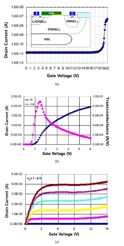
The conventional active-type N-LDMOS device uses a thickness of 30 nm for the high-voltage gate oxide, and it also has a relatively high threshold voltage (Vth) of 1.3 V with the self-aligned diffused channels by means of a diffusivity difference between boron and arsenic. The device is a basic high-Vgs LDMOS that fully operates under a gatesource voltage of Vgs = 12 V. If the device is operated under a gate voltage of 3.3 V or 5 V, which is the logic operation voltage, it does not fully operate because the gate voltage is lower than Vgs = 12 V, and a problem then arises because of a large increase in Rsp. Accordingly, a low-Vgs LDMOS structure is proposed, which fully operates under the logic operation voltage (3.3 / 5 V). This is implemented by controlling the thickness of the logic gate oxide with 7.8 nm (3.3 V) or 12 nm (5 V) so that the logic operation voltage becomes the condition of the gate voltage. Furthermore, in order to prevent a drop in Vth caused by the reduced thickness of the gate oxide, five, or more, times the normal diffused channel concentration of boron and arsenic is applied to fabricate a low-Vgs N-LDMOS with a logic operational Vth. This enables a direct interface between the CMOS and the LDMOS. However, application using this thickness for the logic gate oxide results in a high electrical field on the drain side, so that the breakdown voltage is lowered. Normally, to address this problem the breakdown voltage would be raised by increasing the gate-to-drain distance [7], but this brings about another problem of increased Rsp values. Therefore, in this study a double gate oxide is applied to the drain side in order to solve the problem of the decreased breakdown voltage. Doing this makes it possible to have a high breakdown voltage while maintaining the maximum driver current gain, which allows for the implementation of a low-Vgs N-LDMOS with a low Rsp. The inset in Fig. 1(a) shows the structure of an NLDMOS device to which a double gate oxide is applied. In order to develop a low-Vgs LDMOS device, various low- Vgs N-LDMOS devices have been evaluated and produced by modifying the diffused channel concentrations of boron and arsenic and applying a double gate oxide to improve the Rsp and increase the level of the breakdown voltage. The devices are evaluated with various test patterns, manual measurement data, and via simulations, and the resulting PCM data is then analyzed.
When the low-Vgs N-LDMOS is tested at Vgs = 5 V with a 12-nm logic gate oxide for a 5 V operating logic gate voltage, most of the electrical characteristics are good, but the breakdown voltage of the N-LDMOS device at Vds = 12 V does not give a sufficient margin. The lower limit for the
breakdown voltage should be at least 15 V, but is found to be about 13.7 V, which too low. In order to obtain an additional margin of the breakdown voltage of the above NLDMOS device, the distance of the gate-to-drain is increased from 3.4 ㎛ to 3.6 ㎛, and by doing so it has been found that the breakdown voltage margin is improved to more than 18.2 V, but the increased distance causes the
Rsp to worsen, increasing it from 16.2 to 22.2 mΩ·mm2. It is a general phenomenon that trade-off is exhibited between breakdown voltages and Rsp. This is because a large electrical field is formed on the drain side. The distance of the gate-to-drain is increased in order to disperse the large electrical field on the drain side, but this is not ideal because it results in a poor Rsp (that is, in increased Rsp values). Thus, in order to improve the breakdown voltage without increasing the distance of the gate-to-drain, it is proposed to create a structure of low-Vgs N-LDMOS with a double gate oxide. The electrical characteristics of the low-Vgs NLDMOS with the double gate oxide at Vgs = 5 V are shown in Fig. 1.
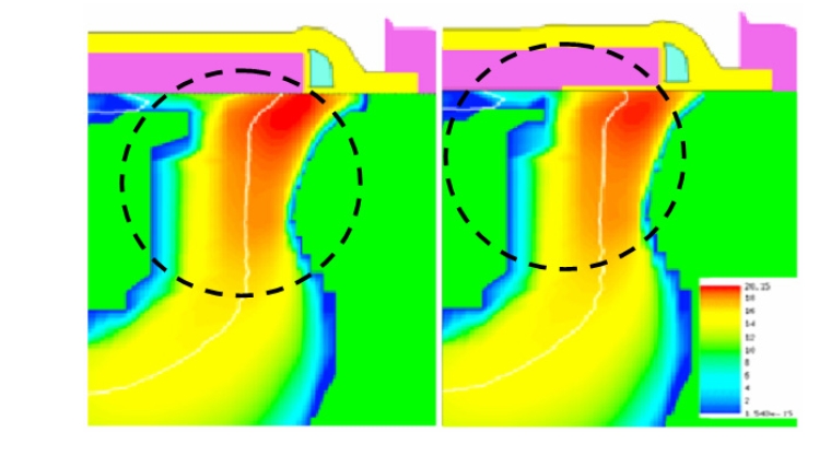
All of the electrical characteristics are considered to be good. In particular, a conventional N-LDMOS device has a breakdown voltage of about 13.7 V, which does not give a sufficient margin, but the application of the double gate oxide results in a stable level at 20.0 V. The Rsp of 15.1 mΩ·mm2 is an even better value than that found in conventional N-LDMOS elements. That is, the breakdown voltage is higher with better Rsp than in conventional or improved breakdown voltage situations because the breakdown voltage is made sufficient by the application of the double gate oxide, which can withstand the formation of the excessive electrical field on the drain side. This corresponds to the simulation results as shown in Fig. 2.
A structure and a process for optimizing the low-Vgs LDMOS device by applying a double gate oxide have been presented. Both the breakdown voltage and the Rsp are improved because an excessive electrical field is formed on the drain side. This will be beneficial in optimizing the power efficiency and size effectiveness for low-Vgs LDMOS devices to which a direct interface can be implemented between the CMOS and LDMOS devices in order to minimize the chip area.