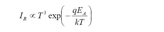
The leakage current in logic devices is one of the most important factors influencing their power consumption. Some research groups have investigated various leakage components in the fabrication processes, including the thickness of the cobalt (Co) salicide, the source and drain scheme, and the shallow trench isolation (STI) profile [1]-[3]. To measure the leakage current effectively, it is necessary to use larger test patterns that include a variety of components at the wafer areas, peripheries, and corners, rather than simply testing the transistors. It is particularly important to control the leakage current, because of its effect on the image quality through the presence of dark noise in a CMOS image sensor (CIS). Various ideas have been suggested for reducing the dark leakage current related to the photodiode structure and pixel schemes [4]-[6]; however, these studies did not take into account the process variation of the STI step height, because the junction was located at a sufficient depth from the silicon (Si) surface. When the source and drain regions in a transistor each have a contact region with the STI, the STI step height has no significant effect, due to the high implantation energy and dopant dose; however, the STI step height in CIS devices may act as a source of leakage in the photodiodes, due to the nitride stringer size after the sidewall etching. In order to analyze the effect of nitride stringers on the image quality, we used test patterns with different perimeter lengths and we also analyzed the effects of boron implantation under the silicon surface.
We fabricated new test patterns and a CIS with a pixel size of 2.5 x 2.5 μm with standard 0.16-μm CMOS logic using a single poly-3 metal process. Red and green photodiodes were formed by epitaxial growth and continuous dopant implantation before the formation of the active region. Blue photodiodes were fabricated by implantation after the formation of the gate-poly. After the photodiode processing was complete, 0.18-μm CMOS logic ICs were fabricated for the purpose of transferring the signal. Finally, we formed a micro-lens for the purpose of gathering more light into the pixels. Normal transistors in a logic device are generally constructed with source and drain regions that are made with a high implantation energy and dopant dose. In this case, these regions were produced after the formation of the poly-gate sidewall. The process used for making the sidewall also forms nitride stringers on the edge of the STI. If they are large enough to cover the active region, they can interrupt the implantation of the dopant into the silicon.
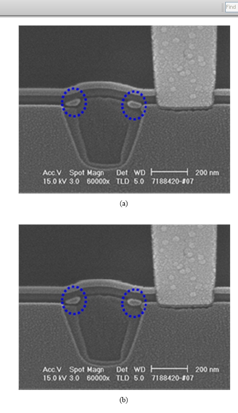
However, in this case, this is not a problem, because both the implantation energy and dopant dose are very high. Therefore, the nitride stringers at the edge of the STI do affect the doping profile in a normal transistor. In the case of the photo pixel array, the process of fabricating the photodiode is as follows: Arsenic dopant (n-type) was implanted into the p-type doped silicon. After forming the poly gate and the sidewall, boron was implanted to form the diode junction in silicon. During this process, the implanted boron density under the overlapped region between the nitride stringer and the active region is insufficient. We hypothesized that this would cause problems with the real display images of the sensor. Therefore, various experiments were conducted to confirm the influence of the nitride stringers on the real display images. To accomplish this, we formed STI steps with two different heights during the STI CMP process. Figures 1(a) and 1(b) show the structures with the different nitride stringers. Figure 1(a) is a cross-sectional scanning electron microscopy (SEM) image of the good structure with the suitable nitride stringer. Figure 1(b) shows the cross-sectional SEM image of the structure with the
nitride stringer that is too large. We investigated the performances of these different structures.
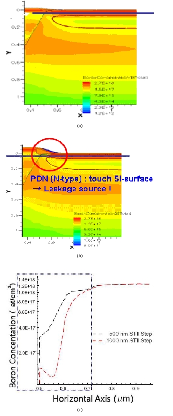
Figures 2(a) and 2(b) show the doping profiles of the two samples. Figure 2(c) provides a comparison of the different boron densities under the silicon surface. From the simulation results, a distinct difference was found between the two samples near the edge of the STI, with the boron density controlled by the large nitride stringer being lower than the baseline condition in Fig. 2(a).
This implies that the doped arsenic rose up near the region overlapped by the large nitride stringer and that the electrons, which are majority carriers of the n-type dopant, moved onto the silicon surface without restraint. This is what caused the dark leakage current.
[Table 1.] Activation energy as a function of diode junction type in pixellike structure.
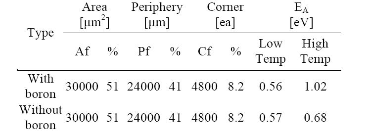
Activation energy as a function of diode junction type in pixellike structure.
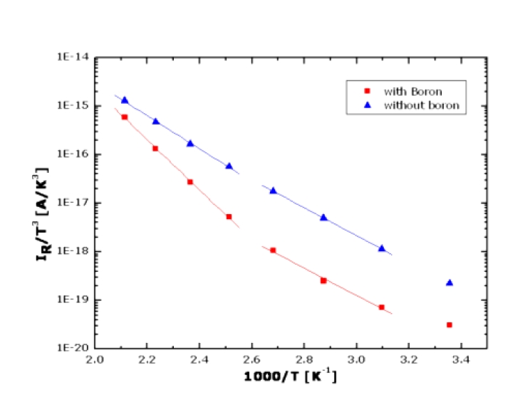
In order to analyze the dark leakage current created by the excess electrons moving onto the silicon surface, we fabricated test patterns with different perimeter lengths. These patterns consist of areas, peripheries, and corners, as summarized in Table 1. As shown in Fig. 3, an Arrhenius plot was used to confirm the electron effect under the silicon surface. An Arrhenius plot shows the logarithm of a rate plotted against inverse temperature. This plot gives us information about the activation energy and the preexponential factor. The Arrhenius equation given as
can be written equivalently as:
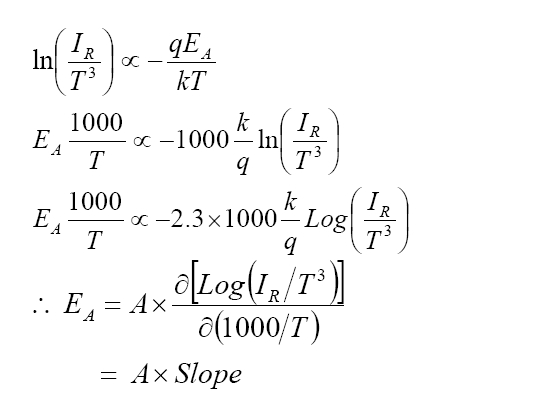
Where A= -2.3 x 1000 x k/q= -0.198375. In general, for high temperatures the activation energy (EA) calculated from the slope of the Arrhenius plot is similar to the silicon band gap. For low temperatures, it is almost half of the silicon band gap. If the activation energy is similar to the band gap energy (Eg), the diffusion current is the major factor in the dark leakage current. If the activation energy is half of the band gap energy (EA=Eg/2), the dark leakage current takes place by generation current and recombination current. When the activation energy is smaller than half of the band gap energy (EA<Eg/2), the dark leakage current is explained by the Poole-Frenkel barrier lowering mechanism. There are distinct differences between the two cases, and the anomalous value of the activation energy in the case without boron is as shown in Fig. 3 and Table 1. In the case without boron, the activation energy is 0.68 eV at high temperatures. This value was almost half the band gap energy, which means that there are traps caused by impurities in the interval between the conduction band and the valence band under the silicon surface, and these traps make it easy to flow the leakage current as well.
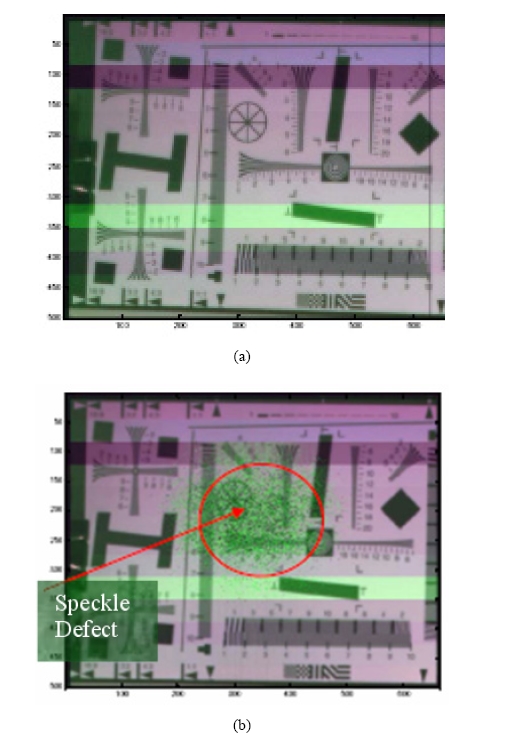
The difference in the real display images was confirmed by using the full array image sensor. As shown in Fig. 4(b), the hot pixels on the real display image were observed, in contrast with the specimen in Fig. 4(a), where the anomaly in the real display is the so-called ‘speckle defect’. We confirmed the speckle defect as an effect of the dark leakage current under the overlap between the nitride stringer and the active region.
In our experimental investigation on the effects of nitride stringers in the CIS, the large nitride stringer brought out the bad boron doping density because of the overlap with the active region. After experiments on the test patterns with different perimeter lengths to confirm the effects of the boron, the probability of electrons moving onto the silicon surface was high, according to the doping density profiles. These electrons caused the dark leakage current from the Arrhenius plots and this in turn gave rise to the speckle defects on the real display image. Consequently, these experimental investigations have confirmed that the nitride stringer at the edge of the STI is a very important factor in the quality of CIS products.