Transparent conducting oxide (TCO) films, such as Sn doped indium tin oxides (ITO) or Al doped zinc oxide (AZO) systems, have been used in various optoelectronic devices such as flat panel displays [1] and photovoltaic solar cells [2]. However, the sheet resistance (Rs) of these TCO films was too high to adapt them as transparent electrodes for improved display applications. Thus, many deposition technologies are being investigated to produce high quality TCO films. ITO/metal/ITO (IMI) [3] and ZnO/Ag/ZnO films [4] are two of the most useful methods for improving the optoelectrical properties of the transparent electrode.
TCO physical vapor deposition methods including reactive magnetron sputtering [5], ion beam deposition [6] and pulsed laser deposition [7] have been reported. Among the methods mentioned, magnetron sputtering is the most frequently used because of this method has high deposition rate on large area substrates, and the film composition can easily be controlled.
Recently, Y. Kim reported that 5-nm thick Au intermediate IMI films were prepared using magnetron sputtering, and these films have better structural and optoelectrical properties than ITO single layer films [8]. However, cost becomes an factor in the production of the ITO and ITO based multilayer films because of the high target cost of Indium (In). Currently, ZnO is a potentially good candidate to replace ITO because of its non-toxicity, low cost, and high stability against hydrogen plasma. Therefore, the structural and optoelectrical properties of the ZnO films deposited with specific impurities, such as Al and Cr, have widely been investigated [9], [10].
The optoelectrical and mechanical properties are important for the application of metal doped ZnO films as transparent electrodes in displays in order to prepare various stress-free transparent conducting multilayer films because the organic light-emitting displays (OLED) devices have one or more layers of TCO films on the substrates.
In this study, ZnO/CuSn/ZnO (ZCSZ) films with a 5 nm thick CuSn interlayer were deposited onto a polycarbonate (PC) substrate using magnetron sputtering in order to fabricate highly transparent and conducting films for flexible optoelectronic devices. Various properties, such as the Rs, optical transmittance and hardness of the ZCSZ film were compared to conventional ITO films.
A sandwich structure of ZCSZ films was deposited using RF and DC magnetron sputtering onto a PC substrate (size; 5×5 cm2) using zinc oxide (7.62 cm diameter) and CuSn targets (99.9% purity, 7.62 cm diameter). The substrate was ultrasonically cleaned in an ethanol-acetone solution for one minute and rinsed with deionized water. Then the substrate was dried with flowing nitrogen gas.
The sputter chamber was evacuated to a pressure 1×10⁻⁴ Pa. The ZnO sputtering was performed in a pure Ar/O2 gas mixture, and the CuSn interlayer sputtering was performed in a pure Ar gas atmosphere. The thicknesses of the ITO single layer and ZCSZ multilayer films were set at 100 and 45/5/50 nm, respectively, by controlling the deposition times. The distance between the target and substrate was 6 cm for all of the depositions.
ITO films with a thickness of 100 nm were also RF magnetron sputter-deposited onto a PC substrate using the same conditions as the ZnO deposition process in order to compare the structural and optoelectrical properties of the two films. Table 1 shows the deposition parameters and conditions for the ZnO and CuSn interlayer.
[Table 1.] The deposition parameters and conditions for the ZnO and CuSn interlayer.
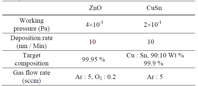
The deposition parameters and conditions for the ZnO and CuSn interlayer.
After deposition, the film thickness and crystallinity were measured using a surface profiler (Alpha-step 500, TENCOR) and X-ray diffraction (XRD, Cu-Kα X’pert Pro MRD, Philips), respectively, at the Korea Basic Science Institute (KBSI). The Rs was measured with four point probes (HMS-3000, Ecopia), and the optical transmittance in the visible wavelength region was measured using a UV-Vis spectrophotometer (Cary 100 Cone, Varian). The bare PC substrates had an optical transmittance of 87%. A nanoindenter (Nanoindenter XP, MTS) was used with a continuous stiffness measurement system to measure the difference in hardness of the ITO and ZCSZ films. The maximum indentation displacement and load were set at 80 nm and 6 mN, respectively. To measure the hardness without effecting the substrate, the hardness was determined using the results measured at an indentation penetration depth of 10 nm and an average of 10 measurements were performed.
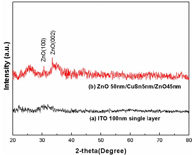
The structural characterization is very important for explaining the optical transmittance and electrical resistivity of the TCO films. Figure 1 shows the XRD pattern of the ITO single layer and ZCSZ multilayer films. For the ZCSZ
films, the diffraction peaks in the XRD pattern were identified as the (100), (002), and (101) planes of the ZnO wurtzite structure.
However, the as-deposited ITO films did not exhibit any diffraction peaks. Similarly, Boehme et al [11] reported that the ITO films deposited using reactive DC magnetron sputtering onto a polymer substrate at room temperature were amorphous. The amorphous XRD pattern of the ITO films in Figure 1 was consistent with Boehme’s study.
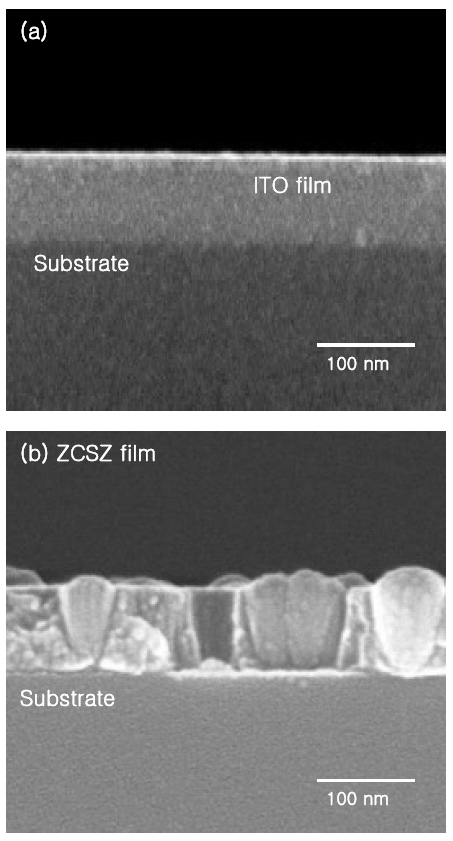
Figure 2 shows the SEM image of cross-sections of the ITO and ZCSZ films. The ITO films did not contain any specific images, whereas the ZCSZ films contained crystallite grains. The grains in the ZCSZ films had a typical cross sectional length of 100 nm. Thompson reported that if the grain size is smaller than the film thickness, normal grain growth occurs [12]. However, normal grain growth in thin films is suppressed by the surfaces and interfaces.
In this study, some grain sizes were larger than the film thickness indicating that abnormal grain growth occurred in the ZCSZ film. However, the reason for the abnormal grain growth in the ZCSZ films is obscure and requires further studies.
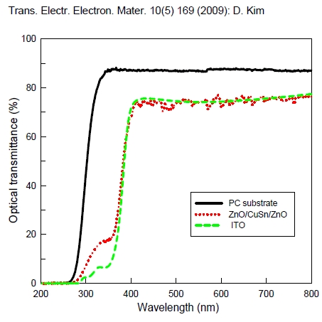
Figure 3 shows the optical transmittance of the PC substrate and the ITO and ZCSZ films in the visible wavelength range of 400 - 800 nm. The bare substrates and the ITO films (containing the PC substrate) exhibited optical transmittances of 87% and 74%, respectively. The optoelectrical properties in this study were similar to the properties that C. Yang et al. reported for ITO films on PC substrates prepared at room temperature using RF magnetron sputtering [13]. Thus, in this study, the properties of the ITO, which were used for comparison to the INI films, were reasonable. Unlike the ITO single layer films, the ZCSZ film was apt to show a lower transmittance because the ZCSZ films had a metallic CuSn interlayer that could absorb visible light. However, the ZCSZ films showed a similar optical transmission of 73% (containing the PC substrate).
Table 2 shows the optoelectrical properties of the ITO and ZCSZ films. In the SEM images, the abnormal grain growth (approximate bamboo structure in Figure 2(b)) was not favorable for the carrier mobility because the bamboo structure had fewer paths for carrier migration. Thus, the ZCSZ films that had an approximate bamboo structure were apt to have a lower mobility than the ITO films. The Halleffect measurements proved that the ZCSZ films did have a lower mobility than the ITO films. Although the ZCSZ films had a lower mobility, the resistivity was lower because of the higher carrier density.
The figure of merit (FTC) [14] is an important index for evaluating the performance of the TCO films. The FTC is defined by the equation FTC = T 10/Rs, where T is the optical transmittance and Rs is the sheet resistance. The FTC for the ZCSZ and ITO films are compared in Table 2. The FTC reached a maximum value at 1.0×10⁻³ Ω-1 for the ZCSZ films, which was greater than the FTC (1.6×10⁻⁴ Ω-1) of the ITO films. Therefore, the ZCSZ films had better optoelectrical properties than the ITO films.
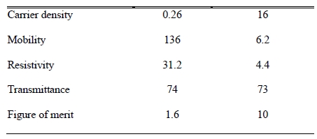
Comparison of the carrier density (´1020/cm3), carrier mobility (cm2/Vs), electrical resistivity (´10-4 Ω cm), optical transmittance (%) and figure of merit (´10-4 Ω-1) of the ITO single layer and the ZnO/CuSn/ZnO multilayer films.
Additionally, the average hardness of ITO and ZCSZ films was compared. The hardness of the ITO and ZCSZ films were determined using nano-indentation and were approximately 5.8 and 7.1 GPa, respectively.
These results showed that the ZCSZ films had the greater hardness than the ITO films deposited under the same processing conditions, suggesting that the ZCSZ films may be advantageous over the ITO films for certain applications.
Transparent, conducting ZCSZ multilayer and ITO singlelayer films were deposited on PC substrates without intentional substrate heating using RF and DC magnetron sputtering.
In XRD measurements, the ZCSZ films showed the ZnO (100) and (002) diffraction peaks, whereas the ITO films did not any diffraction peaks, indicating the synthesis of a crystallized ZCSZ film at a low temperature of 70℃.
The figure of merit measurements, which evaluated the optoelectrical performance of the transparent electrode materials, demonstrated that the ZCSZ films (1.0×10⁻³ Ω-1) were of better quality than the ITO films (1.6×10⁻⁴ Ω-1). The average hardness of the ZCSZ films and ITO films were 7.1 and 5.8 GPa, respectively.
Based on the evaluation of the various properties of the ITO and ZCSZ films, the ZCSZ films were capable of a superior optoelectrical performance compared to the conventional ITO films.