ZnO varistors are multicomponent ceramic devices that exhibit highly nonlinear current voltage (I-V) characteristics and greater energy absorption capabilities [1], [2]. ZnO varistors are essential fir surge protection devices and have dominated the market because of their highly non-linear characteristics. ZnO varistors can generally be divided into two categories, called Bi2O3 -based and Pr6O11-based varistors, in terms of the oxides that induce the nonlinear properties of the varistors [2]. In general, the current-voltage characteristics of the varistors are defined by the power law; I = kVα (k, constant, V, Voltage), where alpha represents the degree of nonlinearity of the conduction. The non-linear characteristic of a ZnO varistor is a grain boundary phenomenon, and the breakdown voltage of the varistor depends on the number of grain boundaries between the electrodes. The electrical characteristics are related to a unit structure composed of the ZnO grain intergranular layer and the ZnO grain in the bulk of the device. The grain size distribution plays a major rule in the electrical behavior. For high voltage applications, a fine grained varistor ceramic is required. Therefore, Sb2O3, Cr2O3, and rare earth oxide (R2O3) are commonly added to control the grain growth of ZnO through the presence of the spinel phase at the grain boundaries of ZnO. Recently, new ZnO varistors with higher varistor voltages (V1mA) have dramatically reduced the size of the varistors. Comprehending the additivesdoping effect on the phase and the electrical properties is very important. Rare earth oxide is often added to the ZnOBi2O3-Sb2O3-Co3O4-MnO2 base varistors with a higher varistor voltage (V1mA). This work investigated the influence of co-doped Y2O3 on the microstructure, the phase, and the electrical and dielectric properties of ZnO-Bi2O3-Sb2O3-CoO- MnO2 -NiO-Nd2O3 system varistors.
Reagent-grade raw materials were used to prepare the varistor with a nominal composition of (95.8-X) mol% ZnO, 0.7 mol% Bi2O3, 1.25 mol% Sb2O3, 0.75 mol% CoO, 0.15 mol% Cr2O3, 0.4 mol% NiO, 0.75 mol% MnO2, 0.2 mol% Nd2O3 and X mol% Y2O3 (X= 0, 0.3, 0.5, 1.0). The mixtures were prepared using ball-milling with zirconia balls in water for 24 h and then calcined at 800℃ for 2 hr. The calcined powder was pulverized using ball-milling with zirconia balls in water. Then a 3 wt% polyvinyl alcohol (PVA) binder was added and the powder was granulated using a spray dryer. The granulated powder was pressed into discs and sintered for 2 hr at heating and cooling rates or 5℃/min in air. The sintered samples were about 10 mm in diameter and 1.8 mm thick. Silver paste was coated on both faces of the samples and, an Ohmic contact was formed for the electrodes by heating at 550℃ for 10 min. The sample microstructures were examined using scanning electron microscopy (SEM, JSM-6360, Joel). The grain sizes were estimated using the linear intercept method. The compositional analysis of the selected areas was determined using an attached X-ray energy dispersive spectroscopy (EDS, Oxford ISIS) system. The crystalline phases were identified using powder X-ray diffraction (XRD, Rigaku, Dmax 2200). The I-V characteristics of the varistors were measured using a high voltage source measure unit (Keithley 237). The varistor voltage (V1mA) was measured at
1.0 mA/cm2, and the leakage current (IL) was measured at 80% of the varistor voltage. Additionally, the nonlinear coefficient (α) was estimated for the current density ranging from 1.0 - 10.0 mA/cm2. The dielectric properties such as the dielectric constant and the dielectric loss were measured with an impedance analyzer (HP4194A, USA).
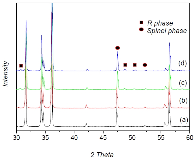
Figure 1 shows the XRD patterns of the ZnO varistors as a function of the Y2O3 amount. The XRD patterns showed hexagonal ZnO as the major phase along with the spinel phase of zinc antimony oxide (Zn7Sb2O12), cobalt antimony oxide (Co7Sb2O12), the pyr℃hlore phase of bismuth zinc antimony oxide (Bi3Zn2Sb3O11) and the R phase (Y2O3 + spinel phase, Y-Sb-Bi-Zn-O). These results suggested that reaction 1 ℃curred at 900℃, and reaction 2 ℃curred above ~ 1050℃ [1].


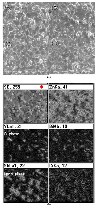
Figure 2 shows the scanning electron micrographs of the fractures and the backscattered electron image of the ZnO varistors as a function of the Y2O3 amount. As the Y2O3 content increased, the average grain size decreased from 6.8 ㎛ to 4 ㎛. These results implied that the addition of Y2O3 inhibited the ZnO grain growth and suggested that the R-phase was segregated at the ZnO grain boundary with Y2O3, and the grain growth was suppressed by the existence of the R-phase with the pinning effect. The mechanism of grain growth inhibition caused by the spinel and pyr℃hlore phases is known for other ZnO based composition with secondary phase forming additives, such as Al2O3, Sb2O3, CoO and others [2]-[4]. Figure 2(b) shows the SEM backscattered electron images doped with 0.5 mol% Y2O3. The Y2O3 rich R-phase and Sb2O3 rich spinel phase were found in the intergranular layer and the nodal point at the grain boundaries of ZnO. Y, Sb, Bi and Zn oxides coexisted in the nodal point and the intergranular layer.
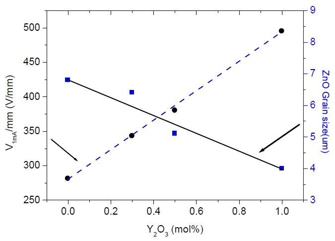
Figure 3 shows the varistor voltage (V1mA) and the grain size of ZnO varistors as a function of the Y2O3 amount. The varistor voltage (V1mA) greatly increased from 275 to 400 V/mm because the decrease in the average ZnO grain size caused an increase in the number of grain boundaries. The varistor voltage (V1mA) is defined using the following equation,

where k is a constant and D is the grain size of ZnO.
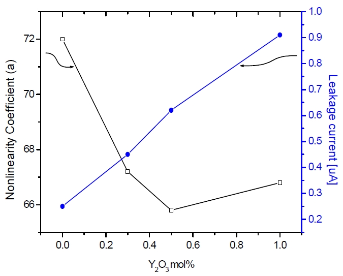
From this equation, the relation between the varistor voltage and average ZnO grain size is inversely proportional. Figure 4 shows the nonlinearity coefficient (α) and the leakage current (IL) of the sample as a function of the Y2O3 amount. The nonlinearity coefficient (α) showed decreased from 72 to 65 with increasing Y2O3 amount. On the other hand, the leakage current (IL) increased from 0.2 to 0.9
Assuming that ZnO formed a solid solution with Y2O3 gives
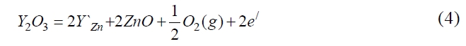
During this reaction, the trivalent Y3+ ion replaced a divalent Zn2+ ion on the lattice through the liberation of a net electron to the conduction band and the formation of positively charged 2Y' Zn. This reaction mechanism assumed that the Y2O3 doping effect on the non-Ohmic properties was related to electronic state at the grain boundary [5], [6].
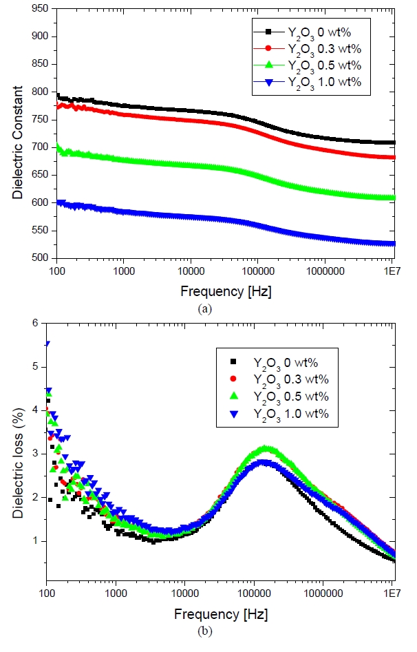
Figure 5 shows the dielectric constant and the dielectric loss with respect to the frequency of the Y2O3 doped ZnO varistor samples sintered at 1150℃. The dielectric constant
is decreased with increasing amounts of Y2O3, which was mainly attributed to the high resistivity of the segregation layers 1.42 [M-ohm]. Interestingly, the dielectric constant produced a peak at a frequency around 100 KHz and decreased again up to 10 MHz. As the frequency increased, the space charge caused the oscillation to lag, producing a Maxwell-Wagner relationship between the varistor, with a time constant (τ) that was dictated by the dielectric constant and resistivity (ρ), and the dimension (d) of grain boundary and the grain. The peak frequency in the dielectric loss is given by fmax ≒ (d1/d2)1/2 (1/2πεoερ2), where the subscript "1" denotes the grain boundary, the subscript "2" denotes the ZnO grains, and ε = 8.5 is the dielectric constant of ZnO. Therefore, the frequency depended on the resistivity [4], [6], [7].
The influence of the added Y2O3 content was investigated in a starting ZnO-Bi2O3-Sb2O3-CoO- MnO2-NiO-Nd2O3 system. In the Y2O3 doped samples, the spinel and R phases (Y2O3 +spinel phase, Y-Sb-Bi-Zn-O) were present at the grain boundaries and played a role in the inhibition of the grain growth. As the Y2O3 content increased, the average grain size decreased from 6.8 α to 4 α, and varistor voltage (V1mA) greatly increased from 275 to 400 V/mm. The nonlinearity coefficient (α) decreased for 72 to 65 with increasing Y2O3 amount. On the other hand, the leakage current (IL) increased from 0.2 to 0.9