Since monolayer graphene was isolated from bulk graphite using a scotch tape and showed the excellent electrical properties, researches on the 2-dimensional (2D) materials have been much attention as a functional material for next generation flexible electronics[1-3]. Recently, large-area (4-inch wafer size or greater) 2D materials with atomic thickness such as graphene (Gr), molybdenum disulfide (MoS2), and hexagonal boron nitride (h-BN) are synthesized on a donor substrate using a chemical vapor deposition (CVD) method, and the large-area 2D materials have been utilized as a conductor, semiconductor, and insulator of flexible electronics[4-10].
In order to utilize the large-area 2D materials for flexible electronic devices, a “transfer process” is required to move the 2D material from the donor substrate to a target substrate. The most common transfer process is wet transfer and dry transfer[11,12]. Wet and dry transfer is generally distinguished depending on the environment in which 2D materials are transferred. In wet and dry transfer processes, a thin polymer film is coated or attached on the 2D material on a donor substrate, and the donor substrate is etched away. Finally, the 2D material on the polymer film is transferred onto a target substrate. In addition, there are direct transfer methods in which 2D materials are electrochemically and mechanically delaminated from their donor substrates without etching of the donor substrate for reuse. The reason why these various transfer processes are proposed is because the transfer of large-area 2D materials from a donor substrate to a target substrate without damages is one of the key technologies for fabricating flexible electronic devices and improving their performance[13-15]. However, high-quality and large-area 2D materials are easily degraded during the transfer process because of contaminations and structural damages of 2D materials. In this reason, many researchers have suggested various transfer methods for reducing the damages and residues from the thin polymer film, and they still tried to solve the problems through mechanical and chemical methods.
In this paper, we introduced the various transfer processes for high-quality and large-area 2D materials. Particularly, we focused on the efforts to reduce the chemical and mechanical damages occurring in transfer process. Moreover, through an understanding of the transfer processes of 2D materials, we propose future research directions for transferring high-quality large-area 2D materials without damages.
2. Transfer of Two-Dimensional Materials
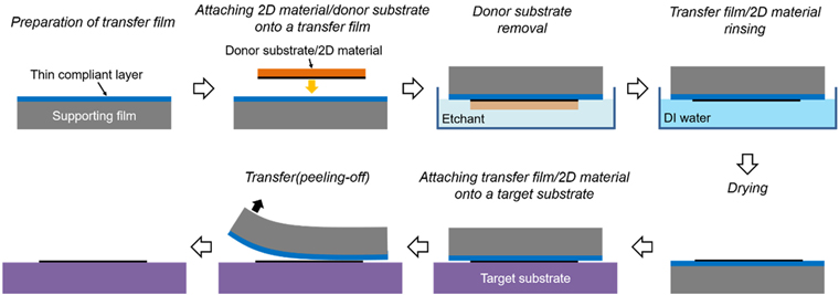
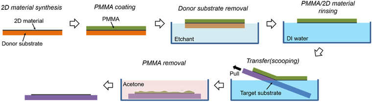
The wet transfer process, which uses polymethyl methacrylate (PMMA) as a transfer film, is the most common transfer process for transferring 2D materials (Fig. 1)[7,16]. In the process, firstly, PMMA is coated onto 2D material synthesized on a donor substrate, and then dipping PMMA/2D material/donor substrate stack in an etchant to etch away the donor substrate. During wet transfer process, PMMA plays a role for protecting 2D material from mechanical damages. PMMA/2D material after removing the donor substrate floats in deionized (DI) water for rinsing residual etchant, and PMMA/2D material floating on DI water is scooped by a target substrate. Then, PMMA/2D material/target substrate is dipped in a solvent for removing PMMA. This wet transfer process has advantages of being able to freely select a target substrate and reduce mechanical damages of 2D material due to the PMMA layer during the transfer process. It was also reported that large-area 2D material with 4-inch wafer size could be transferred onto desired target substrate using the wet transfer process [10,17]. However, PMMA is difficult to be completely removed from 2D material surface. The PMMA residues causes the degradation of the electrical and optical properties of the flexible electronics fabricated with 2D materials[18].
For completely removing PMMA on 2D material, the additional etching or annealing processes at high temperature were suggested to improve the electrical and optical properties of transferred 2D material[19-22]. Furthermore, the methods such as surface treatment on PMMA and the concentration control of solvent were suggested as well[23-27]. However, these wet transfer processes are not only too complex, but also limited in the materials selection of a target substrate. Above all, the residual PMMA is not perfectly removed in spite of the additional methods.
To solve the problem of PMMA residue on 2D material, the various polymer such as 2-(diphenylphosphory) spirofluorene (SPPO1)[28], pentacene[29], polyvinyl alcohol (PVA)[30], polycarbonate (PC)[31] were used as a transfer film instead of PMMA in wet transfer process. Nevertheless, the polymers are not easily removed due to its strong chemical bonding with 2D material and cause chemical doping of 2D material which means that optical and electrical properties of transferred 2D material are degraded. SPPO1 doesn’t leave residue on 2D material, but it’s too brittle to be fragile which means that SPPO1 is not suitable for wet transfer process of large-area 2D material. Recently, it was reported that a residue-free wet transfer process for 2D materials was possible to use rosin[32] and paraffin[33], and some high performance of flexible electronics with residue-free 2D material was demonstrated. However, the wet transfer processes using rosin and paraffin film have still disadvantages that they require additional solvent processes to remove residues, and that the area of transferred 2D material is smaller than that of wet transfer process using PMMA.
The development of the wet transfer process introduced above has enabled to minimize mechanical and chemical damages of high-quality 2D materials with several centimeters size. However, the wet transfer process has limitations that it can cause wrinkles in transfer film/2D material stack when scooping the stack in floating in liquid by a target substrate, and that it was difficult to continuously transfer 2D materials with tens of centimeters size. In order to overcome the limitations, researches on residue-free transfer films allowing large-area continuous transfer process are required in future.
Dry transfer process was suggested for large-scale transfer process using the adhesion difference in transfer film/2D material and 2D material/target substrate interfaces. In other words, the adhesion between 2D material and a target substrate should be greater than that between 2D material and a transfer film for transferring 2D material without damages. Therefore, the adhesion of transfer film/2D material interface should be large enough to support 2D material from damages by external forces, but less than the adhesion of 2D material/target substrate interface.
Polydimethylsiloxane (PDMS), which is a representative viscoelastic material with the water contact angle of about 100° to 110°, was used as a transfer film for dry transfer process of 2D material[4,34,35]. However, there is a problem that 2D material cannot come into contact with PDMS uniformly because the surface of 2D material/donor substrate is not ideally flat due to the grain boundary of a donor substrate and the ripple patterns formed on a donor substrate during the synthesis process of 2D material[36,37]. In addition, because PDMS supports 2D material with a weak Van der Waals force (VdW), mechanical damages on the 2D materials could be easily generated in etching and rinsing processes, resulting in degraded electrical and mechanical properties of 2D material. Moreover, 2D material is not partially transferred from a transfer film to a target substrate because the adhesion difference between two interfaces is not large.
The disadvantages of PDMS was solved by using a thermal release tape (TRT) as a transfer film in roll-based dry transfer process of graphene with 30-inch size, and a flexible touch panel was demonstrated with the transferred graphene[38]. The results showed the potential for integration of 2D materials into flexible electronic devices in an industrial aspect. Then, hot pressing method was suggested to uniformly press TRT/graphene stack onto a target substrate in dry transfer process, and the electrical properties of graphene was improved comparing to previous works[39]. In addition, the performance of electronic devices was demonstrated in laboratory scale with 2D material transferred with self-release layers (SRL) such as polyisobutylene, polystyrene, and teflon [40]. The dry transfer processes using TRT or SRL film have the advantage of being able to continuously transfer large-area 2D materials onto a desired target substrate. However, there is the disadvantage that the adhesives inside TRT or SRL leave residues on 2D material surface after dry transfer process.
To minimize the residue on 2D material in dry transfer process, a transfer film composed of a Si-based thin compliant layer and a supporting film was applied to dry transfer process (Fig. 2)[41]. The transfer film is pressed to induce conformal contact between the compliant layer and 2D material, and the supporting film not only prevents excessive deformation of the compliant layer during dry transfer process, but also helps to easily handle large-area 2D material/transfer film structure in roll-based dry transfer process[42,43]. Later, the transfer film composed of a Si-based pressure sensitive adhesive (PSA)/supporting film, which can be more conformally contacted with 2D material and reused, was developed to enhance the electrical properties of 2D material after dry transfer process[44]. However, there is a limitation that 2D material is not partly transferred onto target substrate because the adhesion difference between a transfer film/2D material interface and a target substrate/2D material interface is not still large. Thus, there is still challenges to achieve the large adhesion difference at the interfaces and use a target substrate with low adhesion to 2D material.
Dry transfer process of 2D material can be easily applied to roll-based transfer process for continuous and large-area transfer of 2D material, which has great advantages in terms of industrial utilization. However, the mechanical damages of 2D material during dry transfer process still occur easily. To solve the problem, it is important to control the adhesion of transfer film, which enables the damage-free transfer of 2D material.
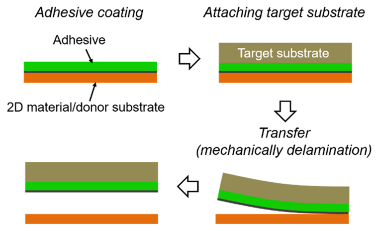
Mechanical transfer process is the transfer process of mechanically delaminating 2D material from a donor substrate without removing a donor substrate for reuse (Fig. 3). Therefore, the strong adhesion between 2D material and adhesive is required to delaminate 2D material from the donor substrate.
Adhesives mainly used in mechanical transfer process are thermoplastic or thermosetting adhesives such as ethylene-vinyl acetate (EVA)[45-47], polyvinyl alcohol (PVA)[48-52], and epoxy[53-55]. In the cases of thermoplastic adhesives, the adhesive conformally contact with 2D material on donor substrate at high temperature and pressure, and then adhesive/2D material peeled off from the donor substrate at room temperature. In the cases of thermosetting adhesives, the adhesive is coated onto 2D material on a donor substrate in a viscous state, and thermally cured to strongly adhere to 2D material. Then, the cured adhesive/2D material is delaminated from the donor substrate. Until recently, various mechanical transfer processes of 2D material for fabricating high performance flexible electronics have been demonstrated[47, 51, 52, 55].
The mechanical transfer process has great industrial and economic advantages because it enables continuous large area and roll-based transfer process using commercial adhesives. In addition, because donor substrates are not removed during the mechanical transfer process, it can be reused for the synthesis of 2D material. However, some serious problems still remain in the process. The 2D material adhered on adhesives cannot be transferred onto a desired substrate again. In addition, the 2D material can be easily torn during the process which mechanically delaminates 2D material from a donor substrate, and the damages reduce the electrical quality of 2D material.
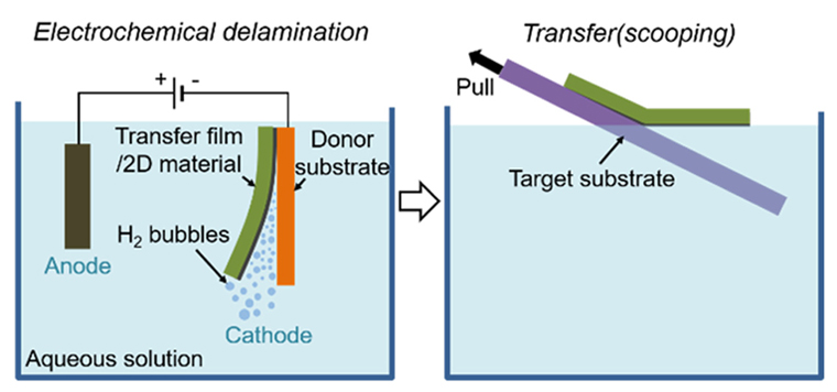
The electrochemical transfer process, commonly called bubbling transfer process, is a method of delaminating 2D materials from a donor substrate using hydrogen bubbles generated at the interface between 2D material and a donor substrate by a reduction reaction of aqueous solution according to the voltage applied to anode and 2D material/donor substrate (cathode) (Fig. 4)[52, 56, 57]. In this case, a transfer film such as PMMA are used to support 2D material being delaminated form a donor substrate, and then transfer film/2D material stack floating in the aqueous solution is scooped onto a desired target substrate such as wet transfer process. Compared to the typical wet and dry transfer process, which takes a long time to remove a donor substrate, electrochemical transfer process is quick to delaminate 2D material because the donor substrate is not removed for reuse. However, 2D material is torn partly by the bubbles generated during the process.
Bubble-free electrochemical transfer process is proposed to prevent the damages caused by the bubbles[58,59]. Whereas the conventional electrochemical transfer process uses a reduction reaction of aqueous solution, the bubble-free electrochemical transfer process uses a reduction reaction of the native oxide layer on donor substrate. In other words, the native oxide layer of donor substrate is reduced at an energy level lower than the energy level at which the solution begins to be hydrated, thus it prevents to generate hydrogen bubbles from aqueous solution. For this reason, the damaged area in 2D material after the bubble-free electrochemical transfer process was 0.32 ± 0.2% in total area of 512 × 490 µm2 which showed significant enhancement compared to the damages area of 6.9 ± 5.7% after the conventional electrochemical transfer process[58]. However, the bubble-free electrochemical transfer process has disadvantages that the process time takes long compared to the conventional electrochemical transfer process, and applicable donor substrates are limited.
The electrochemical transfer process has great advantages in industrial aspect because the donor substrate can be reusable and the process can be applicable to a roll-based continuous transfer process. However, the electrochemical transfer process leads mechanical damages in 2D material by the bubbles generated at the interface between 2D materials and metal substrate, and the bubble-free electrochemical transfer process is too slow to reduce the process time. In addition, it is difficult to completely remove the coated transfer film on 2D material as well as mechanical damages such as wrinkles as the conventional wet transfer process.
The transfer processes introduced above use polymer transfer films or adhesives to transfer 2D material to a target substrate, and the disadvantages such as polymer residues have been continuously mentioned. Therefore, various “polymer-free” transfer processes without transfer films or adhesives were proposed to prevent the polymer residues[60-63]. For the conformal contact between 2D material and a target substrate, the 2D material on donor substrate was adhered to the target substrate by electrostatic force, and then the donor substrate was etched away in etching solution[60]. It was also proposed that 2D material was transferred directly from a donor substrate to a target substrate using a frame[61,62], and a hexane-assisted wet transfer process without a transfer film was suggested[63].
These transfer processes have the advantage of residue-free transfer. However, because there are no transfer films or adhesives that support 2D material, it is difficult to transfer them in large areas and continuously. In addition, 2D material can be easily torn during the transfer process.
3. Future Challenges & Perspective
In this review, the research trends on transfer process of 2D material were discussed. Table 1 outlines the 2D material used in each transfer method and their advantages and disadvantages. The transfer processes of 2D material have been steadily developed through mostly mechanical and chemical approaches. However, despite of the development of various transfer processes, it still seems to require a lot of research and development on large-area damage-free transfer process of 2D materials for commercializing 2D material-based applications.
[Table 1.] Representative transfer methods for two-dimensional materials
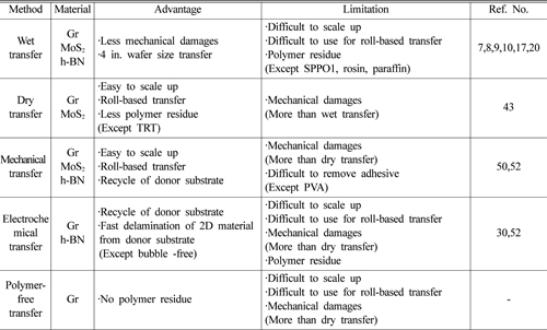
Representative transfer methods for two-dimensional materials
Mechanical and electrochemical transfer processes are etching-free transfer processes with the advantage of being able to reuse a donor substrate. Recently, the electrochemical transfer process combined with the mechanical transfer process was performed on a roll-to-roll basis using EVA film[64]. The advantages of mechanical and electrochemical transfer processes showed the potential for industrial utilization of etching-free transfer process. However, polymer residues and mechanical damages are still caused during the etching-tree transfer process. Various attempts to solve the problems are being tried in multiple ways, but the use of strong adhesives to prevent tearing of 2D material is still a challenge.
Wet transfer process, most commonly used in transfer of 2D material, has great advantages in terms of electrical quality of transferred 2D material compared to the mechanical and electrochemical transfer processes. In addition, the problem of polymer residue remaining on 2D material after wet transfer process has been improved. However, the wet transfer method is fundamentally disadvantageous to the large-area and continuous transfer process because the 2D material with a nanometer thickness should be floated in DI water to be scooped by a desired substrate Therefore, an advanced wet transfer process to overcome the disadvantages should be developed further.
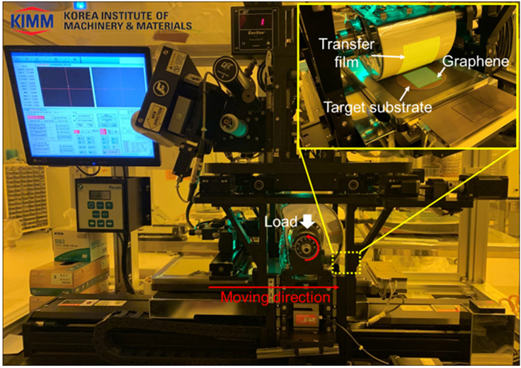
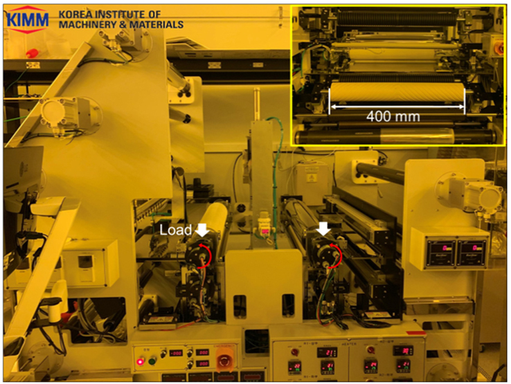
Dry transfer process of 2D material is the most suitable process for industrial aspect compared to other processes because it is easy to apply to continuous transfer of large-area 2D material using a roll-based system. In 2010, the graphene-based touch-screen panel was demonstrated by transferring 30-inch graphene into a flexible substrate through continuous roll-based transfer process with transfer film, which showed that the roll-based dry transfer of 2D materials is practical in industrial use. Since 2012, Korea Institute of Machinery & Materials (KIMM) has been conducting dry transfer process of large-area 2D material using roll-based systems such as “Roll-to-plate” (Fig. 5) and “Roll-to-roll” (Fig. 6). In 2017, Jang et al. in KIMM investigated the damage mechanism that graphene is torn by contact load during the roll-based dry transfer process and improved the electrical properties of dry transferred graphene[65]. In addition, Yoon et al. in KIMM reported that graphene transferred by dry transfer process was not conformally attached on a target substrate comparing to graphene transferred by wet transfer process[66]. Nevertheless, there is still a problem that the electrical quality of 2D material is degraded due to the mechanical damages, and there is not enough research to clearly analyze the mechanism on the mechanical damages of 2D material.
Most of the damages in 2D materials in the various transfer processes introduced in this paper are caused by contact and adhesion at the interfaces of 2D material/transfer film or 2D material/target substrate. Researches related to the transfer film with optimal materials are required to solve the chemical damages such as polymer residue and doping. In addition, the researches on the mechanical design of transfer film are required considering for a continuous transfer process of large-area 2D material. Particularly, in the case of dry transfer process, the compliant layer of a transfer film that makes direct contact with 2D material has a significant effect on the mechanical damages in 2D material. Therefore, it is necessary to investigate the adhesion characteristics, viscous behavior, and mechanical deformation of the compliant layer during the dry transfer process. The studies will be the foundation of large-area damage-free transfer process of 2D materials for industrial use.