A substrate integrated waveguide (SIW) is a well-known type of planar formed waveguide on a printed circuit board (PCB). An SIW is formed with two parallel metallic via holes or grooves in the PCB. Compared with traditional, bulky waveguide, an SIW provides easy-to-fabricate structures, small-sized circuits, and good integration with planar circuits. Studies have already developed various passive and active SIW circuits and devices [1–10]. Of these active SIW amplifiers [1–4] are complicated to design because the signal and ground of the SIW are electrically shorted by metalized via holes or grooves, and they need input and output impedance matching as well as mode conversion circuits between the amplifier and the SIW. A mode conversion circuit, also called the transition structure between the SIW and the planar transmission lines—microstrip (MS), coplanar waveguide (CPW) or conductor-backed coplanar waveguide (CBCPW)—is needed because the SIW and planar transmission lines have different mode characteristic.
An X-band SIW amplifier using a DC-decoupled transition structure between the SIW and the MS was firstly proposed [1]. However, the DC-decoupled transition structure has to be designed very carefully, because the mode and impedance matching properties are very sensitive to the coupling factor of the DC-decoupled transition. SIW power amplifiers using CBCPW-to-SIW and MS-to-SIW transitions were proposed to realize an input/output matching network in the SIW [2,3]. However, it is hard to tune the matching network after PCB fabrication, and the transition length between the SIW and the CBCPW or MS remains long. Note that the long transition structure may cause unwanted coupling and radiation around the circuits [7]. A corrugated SIW distributed amplifier was also reported; however, its performance was not optimized [4].
This study proposes a half-mode SIW (HMSIW) amplifier using HMSIW-to-MS lumped-element transition. The proposed structure was developed using an HMSIW platform that reduces the SIW structure size by half, and it supports the TE0.5,0 half-mode [8]. The lumped-element transition structure was realized using a surface mount technology (SMT) inductor and capacitor to reduce the length of the conventional transition structure [9,10]. The proposed structure is easy to design and enables tuning of the amplifier input/output matching network by using lumped-element transition after PCB fabrication.
II. HMSIW TRANSITION TO MICROSTRIP AND HMSIW AMPLIFIER DESIGN
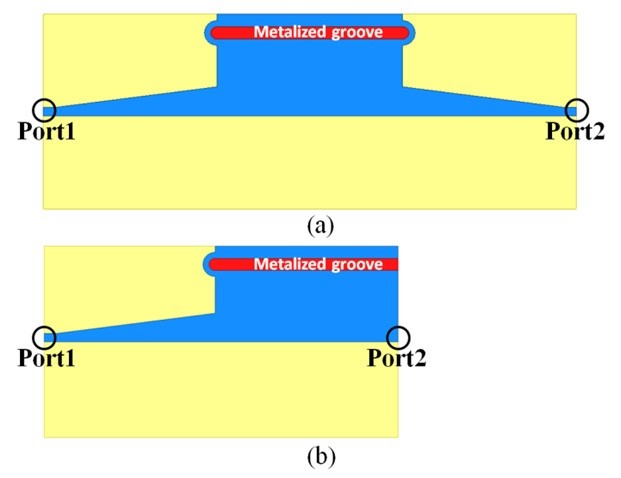
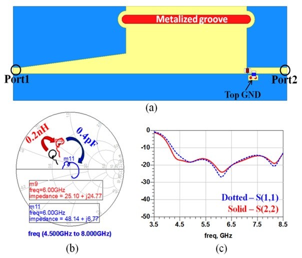
Fig. 1(a) and (b) show the conventional and incomplete transition structures, MS-HMSIW-MS [5] and MS-HMSIW, respectively, on the Taconic TLX substrate (dielectric constant = 2.55, height = 0.508 mm). These transition structures were verified by simulation using ANSYS HFSS ver. 14. Note that ports 1 and 2 in Fig. 1(a) and (b) were excited as a 50-Ω lumped port, and not a wave port in the HFSS simulation.
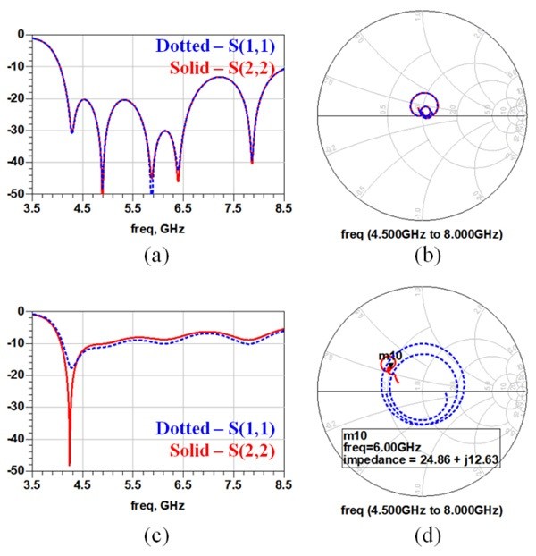
Fig. 2 shows simulation results of the MS-HMSIW-MS and MS-HMSIW structures. In Fig. 2(a), the simulated return losses of the MS-HMSIW-MS are under -15 dB from 4.13 to 6.8 GHz, and in Fig. 2(b), the MS-HMSIW-MS structure shows good matching at 50 Ω from the Smith chart. Note that the simulated HMSIW length is λc/4 ≈ 30 mm. Fig. 2(c) shows the simulated return losses of the incomplete MS-HMSIW transition. However, the incomplete transition structure shows return losses of around -8 dB at ports 1 and 2 because the port-2 impedance is not located on 50 ohm. The port-2 impedance is located at 24.86 +
Murata SMT 0.2 nH series inductor with 0603 mm2 size and a 0.4-pF shunt capacitor were used between the HMSIW and the MS, as shown in Fig. 3(a). Note that the shunt capacitor is bridged with the MS-edge and the extended top-grounded metal pad. The 0.2 nH series inductor moved the 24.86 +
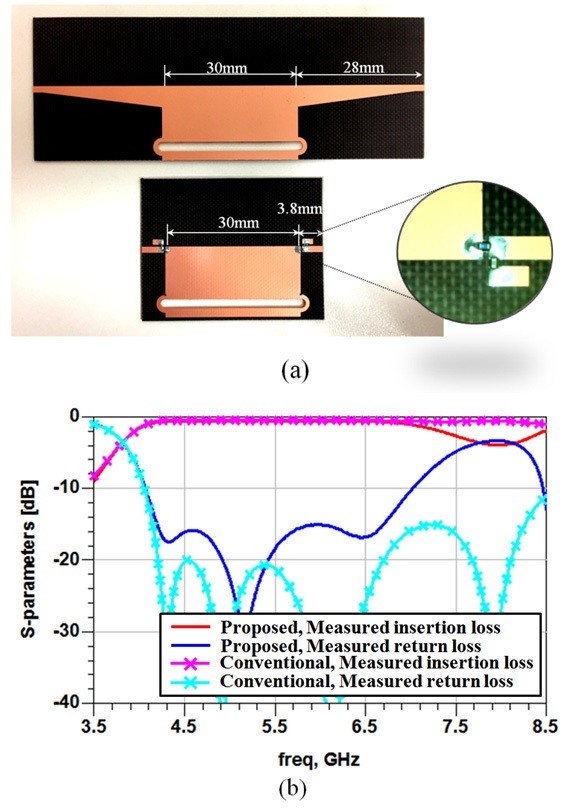
The back-to-back transitions of conventional [5] and lumped-element transition [9] structures were designed and compared to verify the performance, as shown in Fig. 4(a) and (b). The lumped-element transition has a short transition length compared with the conventional transition, as shown in Fig. 4(a). The 0.2 nH series SMT inductor and 0.4 pH shunt capacitor were attached on the matching section. SMA connectors were soldered to the edge of the MS line for the measurement. The measurements were conducted using the Agilent N5230A vector network analyzer. Fig. 4(b) shows the measured Sparameters of the conventional and lumped-element transition structures. The measured insertion loss of the lumped-element structure remains within 0.7 dB from 4.15 to 6.88 GHz. The measured return loss is below -15 dB from 4.2 to 6.7 GHz. The return loss bandwidth of the lumped-element transition structure is narrower than that of the conventional structure because lumped-element matching provides a narrower bandwidth than distributed matching of the tapered line [11]. However, the lumped-element transition structure provides a physically short transition length and shows insertion loss similar to that of the conventional structure in the pass-band.
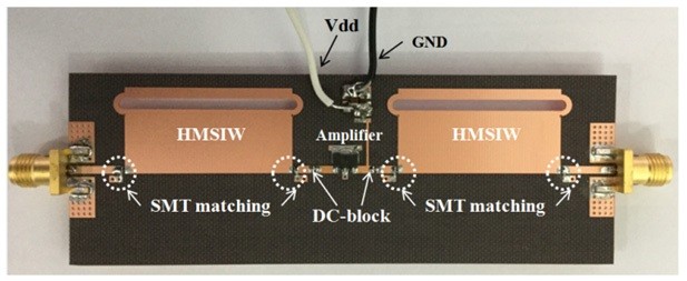
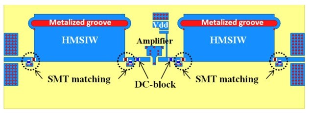
Fig. 5 shows the proposed HMSIW amplifier design and its building blocks. The amplifier is bridged with the HMSIW through the SMT matching section, which plays a role in the HMSIW-to-MS transition and input/output matching networks of the amplifier. Mini-circuit GALI-33+ amplifier was implemented to demonstrate the proposed HMSIW amplifier, and the input and output of the amplifier have 50 pF DC-block capacitors. The input and output impedances of the GALI-33+ amplifier are 50 Ω. Note that if the input/output of the amplifier are not 50 Ω, the input/output impedances of the amplifier should be matched with the HMSIW by changing the values of the lumped-elements.
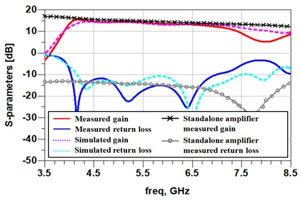
Fig. 6 shows the proposed HMSIW amplifier. This amplifier is biased at 4.3 V with dc current of 45 mA. The proposed amplifier was simulated and measured. Fig. 7 shows the simulated and measured small-signal gain and return loss of the proposedstructure compared with that of the measured stand-alone amplifier. The proposed amplifier has 15 dB gain with 3 dB bandwidth from 4 to 7.05 GHz. The measured return loss is as low as 10 dB from 4.04 to 6.99 GHz. The measured results show good agreement with the simulation results.
This study proposes an HMSIW amplifier with a lumpedelement transition circuit. The lumped-element transition structure has short transition length, and it may reduce the possible radiation to nearby devices compared with the conventional transition structure. The proposed HMSIW amplifier was designed, simulated, and measured. The results indicate that it is promising for small-sized SIW circuit integration.