Wireless communication systems issue various requirements of high mobility, high speed data streaming, huge access capacity, and compact hardware systems. Various approaches, such as multiple access algorithms, system specifications, hardware architectures, and so on, have been studied. Among the system schemes, space diversity using switching beam control is one of the most promising candidates to efficiently increase channel capacity. However, it has the limitations of high antenna complexity and a large form factor of the beam-switchable antennas at mobile terminals [1–4]. An Electrically Steerable Parasitic Array Radiator (ESPAR) antenna has been developed for a compact and simple beam controllable antenna design, and one active element and parasitic elements are used to adjust the beam direction. The ESPAR antenna is a type of reactively steerable array antenna and a single-port array antenna with only one central active element surrounded by several reactively controlled parasitic radiating elements. The ESPAR antenna pattern is controlled by adjusting the reactance load values, including capacitance and inductance [1–6]. The ESPAR antenna has been developed using various parasitic structures, such as monopoles [5], dipoles [6], and patch antennas [7]. However, due to the three-dimensional form-factor, the antenna cannot be integrated with other circuits on a planar substrate. Moreover, as it has only one parasitic element for each direction, its directivity and beamwidth are limited and uncontrollable. An additional parasitic element can increase the antenna gain and front-to-back ratio (F/B), which operates based on the Yagi-Uda antenna [8,9].
In this paper, a new beam-switchable antenna is designed with a planar architecture based on the Yagi-Uda design methodology [2,10,11]. The proposed antenna is able to control bi-directional beams by switching the roles of parasitic antenna elements from reflectors to directors and vice versa. The function of the parasitic element can be changed by adjusting the value of reactance mounted on each parasitic element. Therefore, the proposed planar beam-switchable antenna is designed to operate with bi-directional beam control. Moreover, it has excellent capabilities to achieve a small form factor and to be integrable in planar subsystems.
This paper is organized as follows. Section II describes the proposed antenna architecture. In Section III, the design methodology of the planar Yagi-Uda antenna is explained for the active and parasitic elements, respectively. Section IV presents the implementation and performance evaluation of the proposed antenna. Finally, the feasibility and technical applications are discussed in the conclusion.
Ⅱ. DESIGN METHODOLOGY OF THE PLANAR YAGI-UDA ANTENNA
The proposed beam-switchable antenna is designed with the Yagi-Uda method at 2.4 GHz. Whereas a conventional ESPAR antenna has a single parasitic element for each beam direction, the proposed antenna has additional parasitic antenna elements to achieve higher directivity. The Yagi-Uda array antenna was developed by Uda and Yagi in the 1926 and 1928. The Yagi-Uda antenna consists of several linear dipole elements. Whereas the only one dipole is excited from an RF source called a driven element (active element), the other ones are called directors or reflectors (parasitic element) in which microwave currents are induced by mutual coupling. As the Yagi-Uda antenna is designed to act as a longitudinal array [8,9], the parasitic elements located in beam direction act as directors and those in the opposite side as reflectors.
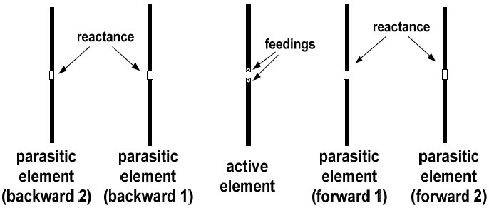
Fig. 1 shows the layout of the proposed planar beam-switchable antenna. The antenna system consists of one active element and four parasitic elements that are arranged with two elements for each bi-direction. The parasitic elements are designed for switchable functions of directors and reflectors. These roles are controlled by changing the reactance of elements. For the purpose of adjusting the element reactance, switchable capacitance is mounted at the center of two monopoles in each parasitic element. The arrangement with flexible directors and reflectors make it possible for the antenna to increase the array antenna directivity and to switch beam directions.
The Yagi-Uda array is designed by adjusting the lengths of the reflectors and directors and the spacing between elements. In general, the lengths of the reflectors are a little longer than those of the directors. The proposed antenna system controls the effective electric length of the parasitic elements. As the number of elements determines the antenna directivity, the array with two directors is efficient for an antenna directivity and an F/B. The number of reflectors is normally not a significant factor that contributes to the antenna directivity. Therefore, the proposed antenna is designed with two parasitic elements for each beam direction under considering the full system form factor. The spacing between antenna elements is optimized at the region of 0.25 λ to 0.4 λ. In general, the element spacing of a quarter wavelength gets about 9–10 dB.
Ⅲ. PLANAR BEAM-SWITCHABLE ANTENNA DESIGN
The active element of the planar beam-switchable antenna is designed with a planar dipole on a FR4 substrate with a thickness of 1.0 mm and a dielectric constant of 4.4. The dipole antenna is aligned on a strip line without a ground plane on the back side, and excited by balanced coaxial feed lines through the back side of the substrate. As the dipole conductor is not aligned in the air, the effective λ/2-dipole is designed, which measures the effective electrical length on an epoxy substrate. The electromagnetic field simulator, HFSS (High Frequency Structure Simulator; ANSYS Inc., Canonsburg, PA, USA) is utilized for the optimum design. The active dipole is implemented with a width of 1.5 mm, total length of 47 mm (0.376 λ0), and separation between monopoles of 2.0 mm; thus 47 mm on the substrate acts as a λ/2-dipole.
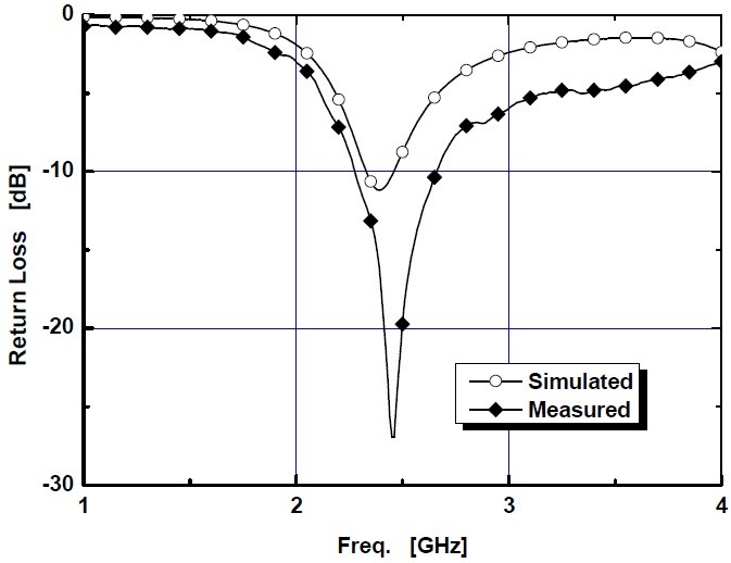
The implemented active element was measured for bandwidths and radiation patterns. Fig. 2 shows the simulated and measured results of the active element. The return loss measured by a vector network analyzer (Agilent E5071C) indicates a center frequency of 2.24 GHz and a bandwidth of 2.10–2.45 GHz, which refers to a return loss of -10 dB. The planar dipole with a length of 0.376 λ0 conducts λ/2-dipole at 2.4 GHz, and thus the physical length of 37 mm is an effective length of λ/2.
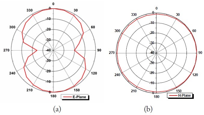
To check the dipole operation of the active element, radiation patterns are measured in an anechoic chamber. Fig. 3 shows the measured radiation patterns for the E-plane and H-plane at 2.47 GHz. From the experimental results, the active element shows omni-directional patterns and a maximum gain of 2.647 dBi.
The parasitic element is designed with controllable dipoles including adjustable reactive components. As the reactive element mounted on a line antenna shortens or extends the antenna length, the parasitic element can switch its role from a director to a reflector or vice versa.
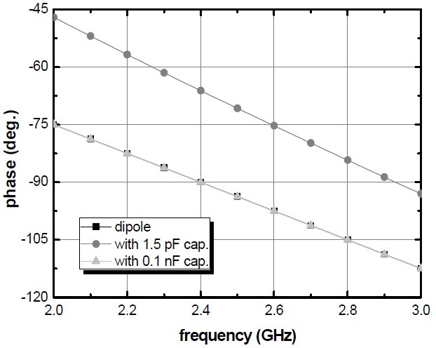
The electrical length is investigated for the values of mounted reactive components using the Advanced Design System (ADS), Keysight Technologies Ltd. Fig. 4 presents the effective electric length of the antenna elements. The electric length variation is searched for the capacitance of 1.5 pF and 0.1 μF, which are compared with the delay of the ideal λ0/2 transmission line. The capacitance is mounted between two λ0/4 striplines. Whereas the parasitic element mounted with a capacitance of 1.5 pF reduces the effective electric length from 90° to 66.15°, the one with a capacitance of 0.1 μF makes the stripline a short-circuited line. The forward-direction parasitic element (director) attains a relatively shorter electric length than the active element by mounting a capacitor of 1.5 pF. The backward-direction parasitic element (reflector) has almost the same electric length as that of the active element with large capacitance. The second parasitic element is designed with a physically shorter electric length of 45 mm compared with that of the first parasitic element at 47 mm. The separation between all antenna elements is set to 37 mm of 0.376 λ0 at 2.4 GHz.
Ⅳ. IMPLEMENTATION AND EXPERIMENTS OF FOUR-WAY BEAM ANTENNA
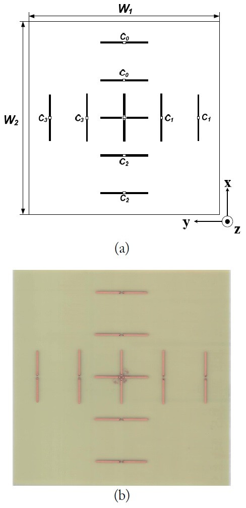
In this section, the four-way beam-switchable antenna is implemented and evaluated with the composite of two bi-directional Yagi-Uda antennas. The orthogonal antenna configuration is presented in Fig. 5. The parasitic elements are arranged for directors and reflectors using the Yagi-Uda antenna methodology. The first and second parasitic elements are designed with lengths of 47 mm and 45 mm, respectively. The distance
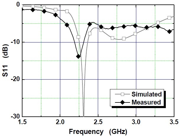
The performances of the proposed planar beam-switchable antenna were experimented and evaluated in an anechoic chamber. To evaluate the performance, return losses, radiation patterns, and beam direction switching are measured. The return losses of the proposed planar beam-switchable antenna are presented in Fig. 6. The center frequency of the planar dipole antenna is 2.3 GHz. The 10-dB bandwidth is 2.2-2.32 GHz. The design results shows that the center frequency shifted by about 0.1 GHz because of the coupling effect between elements.
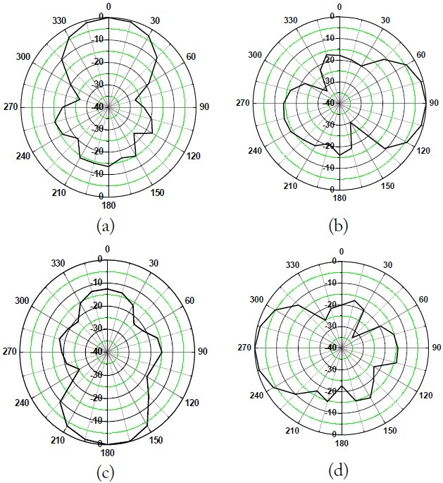
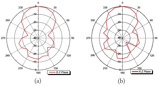
The radiation patterns are measured for the planar beamswitchable antenna on an x-y plane and an x-z plane as shown in Fig. 7. The antenna beam is confirm to align to the 0° direction. The gain presents a maximum gain of 10.74 dBi, a F/B of about 14.7 dB, and a half-power beamwidth of 59.8°. The evaluation of the beam-steering performance is presented in Fig. 8. The gain of antenna in 0°, 90°, 180°, and 270° directions is 10.74, 10.45, 10.67, and 10.7 dBi, respectively. The antenna beam is adjusted by switching the reactance mounted on each parasitic element. From the experimental results, the implemented planar beam-switchable antenna appears to have excellent directivity and beam-steering performance to the desired directions.
In this paper, the planar beam-switchable antenna has been proposed using the Yagi-Uda array design methodology for space diversity applications. The proposed antenna is implemented on a planar substrate with bi-directional beam-switching characteristics, whereas the conventional beam-switchable antenna requires 3-D space. Two orthogonally arranged arrays operate the bi-directional beam switching by adjusting the reactance of the parasitic elements. The measured results verified the beam switching to be aligned to the antenna direction. For a system applied by practical switches and bias lines, a symmetrical and aligned layout and a high isolation of the switch should be considered to maintain proper antenna beam patterns. Therefore, the proposed planar beam-switchable antenna can be implemented in a single fabrication process with other PCB components and is an excellent candidate for mobile wireless communication terminals.