Over the past two decades, a considerable increase has been observed in the demand for wireless communication devices, while the current emphasis has shifted towards more practical consumer applications. As a result, the productivity of such micro devices has increased considerably. Their mechanical switching action makes them superior to other semiconductor switches. Salient features include good linearity, very low insertion loss in the ON state and high isolation in the OFF state while the reliability and power-handling capacity required for these systems are still being improved. These factors have motivated an increased number of studies and modifications in the development of micro-electromechanical systems (MEMS). These devices are termed radio frequency (RF) MEMS which refers to all miniaturized devices; whether their operation is micromechanical, or fabricated by micromachining, or both [1]. The fabrication and design techniques of MEMS systems have significantly improved through the many years of research and experimentation. Due to significant improvements, research on MEMS has gained momentum in the field of microwave systems, and even in optical systems.
Apart from the features mentioned above, these switches also have the advantage of being miniaturized; more importantly, these systems are more efficient than the conventional systems in terms of linearity.
Traditionally, MEMS switches can be divided into two sections: - actuation section and electrical section. The mechanical movement can be achieved using magnetostatic, piezoelectric, electrostatic, or thermal design [2]. Electrostatic actuation is most commonly used because of its small electrode size and virtually zero power consumption. Depending on the design layout, the switches can also move vertically or laterally. The two main types of RF-MEMS switches include the: - fixed-fixed beam and the cantilever beam [3]. Both switches employ varying configurations to be driven in ON state or OFF state. In a series contact switch, the cantilever is fixed at one end, while the other end is free to move; on the other hand, capacitive switches utilize bridge membranes that are fixed at both ends. The operation of a series switch is initiated by applying a bias voltage under the strip which, at the threshold limit, causes the strip to snap down onto the bottom electrode. The opposite tensile force is unable to override the electrostatic force; hence, the cantilever bends down, thereby shorting the input and output t-line, making the switch conductive. In metal shunt switches, the layer of dielectric between the parallel membrane and the t-line forms a capacitor. The switch is driven in the off state by creating a small resistive path between the t-line and ground. For the switch to operate in the ON state, the pull in the voltage is eliminated and an almost complete RF signal is transmitted from the source to the drain.
Research on MEMS is currently being carried out to achieve switches with high tunable characteristics, low loss, high quality factors, small size, low power consumption, and high linearity compared to conventional semiconductor-based passive switches. Due to their many applications, RF MEMS switches have become an extensive area of research [4]. Various MEMS Switches, including the: -Raytheon, Rockwell, Radant and other metal contacts shunt switches have been designed so far. They have evolved into switches with better isolation, lower resistive loss, high power handling capability, and negligible power consumption promising beneficial utilization in many current and future RF spectra and in microwave and millimeter wave systems. The design of the RF MEMS series switches has reached a mature level, with many metal contact switches [5-8] available today.
Stiction problems are efficiently handled by torsional switches, which have wide applications in the field of MEMS and nano-electromechanical systems (NEMS). Many push-pull (see-saw) configuration switches have recently been fabricated, following designs by Hah et al. [9,10], Chiao et al. [11], and Milanovic et al. [12,13], etc. While an existing switch has been designed to operate on a wide RF spectrum, it is limited to 40 GHz [16]. RF MEMS have gained such considerable significance that they are now being integrated with antennas to enhance operation. RF MEMS have been tested for use in reconfigurable RF antennas [17]. This paper deals with a novel metal contact switch that employs a see-saw beam movement mechanism. This liberates the switch of the cantilevers that rely on elastic recovery forces to restore it to its original position when the supply is shut off. The see-saw mechanism makes the switch more reliable with enhanced power handling capacity and low actuation voltage. This novel switch has excellent isolation and almost negligible insertion loss with satisfactory return loss. Moreover, the switch facilitates wide band operations covering 78 GHz bandwidth.
2. DESIGN AND SWITCHING ACTION
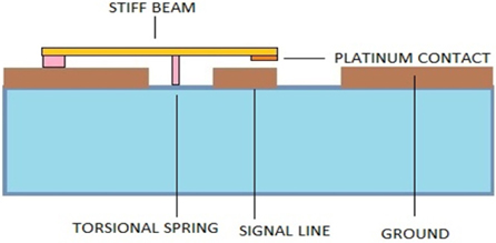
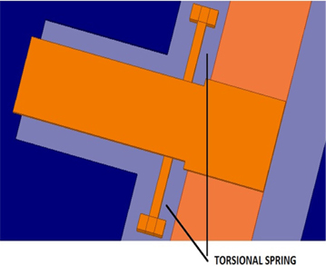
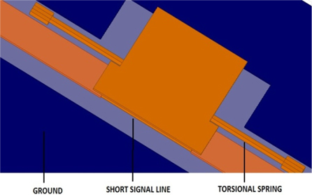
The proposed switch has been designed on a quartz substrate. The switch consists of a coplanar waveguide with a 90 μm signal line and 55 μm gap on either side. The conventional coplanar waveguide (CPW) needs to be modified in order to achieve greater performance [13]. Therefore, the proposed switch was optimized to an impedance of 50 ohm. The signal line is split open and the length of the open signal line is 100 μm. A dielectric was not used as charge injection in the design in order to avoid the charge trapping problem. Charge trapping in dielectrics causes reduction of the restoring force, giving rise to stiction problems. The proposed switch therefore utilizes the operating principles of a metal contact switch to perform its operation. The see-saw beam rests on a torsional spring which is placed over the gap between the grounds and the transmission line. The placement of the torsional spring was made to be unsymmetrical owing to the functionality of the switch. The spring lies more towards the signal line providing a greater portion of beam towards the ground. The design of the see-saw membrane and torsional spring is shown in Fig. 1.
The design will enable ease of contact of the bridge and anchor to the ground (in rest position) when the membrane is liberated from the actuation voltage. The membrane has been designed to be thick to avoid disturbances from mechanical forces such as acceleration, vibration and Brownian noise. The torsional spring facilitates the swinging of the beam making contact with the signal line.
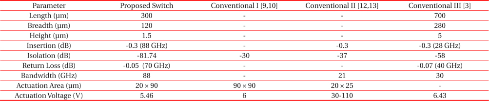
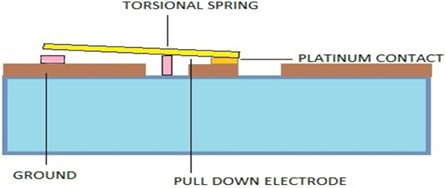
The beam lies in the rest position when no actuation voltage is applied as shown in Fig. 2. In the rest position, the membrane rests over the contact point on the ground; because of this association, the complete signal is transferred to the ground, resulting in high isolation. As soon as the actuation voltage has been applied to the pull down electrode, the beam becomes disassociated from the contact points on the ground and snaps on the transmission line, shorting the signal line that drives the switch to the ON state as shown in Fig. 3. This results in the switch acting as an inline switch. The inductance of the switch can be made independent of the mechanical properties of the membrane and this can be regarded as the main advantage of the inline switch [2]. After the voltage has been removed, the residual stresses pull the switch back to the up-state position. The switch yields excellent performance and RF response than the conventional switches designed by Hah et al. [9,10], Milanovic et al. [12,13] and Tejinder et al. [3]. Table 1 shows a comparison between the proposed and conventional switches.
[Table 1.] Comparison between proposed & conventional switches.

Comparison between proposed & conventional switches.
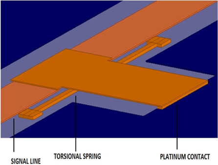
· Contact metal: Unlike the previous switches, in the proposed design the contact metal used is made from thin platinum metal to enhance the reliability of the switch. The contact area between the beam and the signal line was optimised to improve the power handling capability. This also helps to decrease the insertion loss and the overall on-state resistance of the switch. Platinum is harder than conventional contact metals such as gold (Au) and also has a high melting point [14].
· Beam: Earlier switches had a symmetrical beam with respect to the torsional spring i.e. the beam had an equal length on either side [2]. However, in the proposed design, the beam is unsymmetrical having a greater length towards the ground so that when the pull down voltage is removed, the beam automatically descends to the other side (ground).
· In the rest position (as shown in Fig. 2) and in up-state (i.e. when the pull up electrode actuates the beam), the beam did not touch the ground. In the proposed design, when the beam is in the rest position, it makes contact with the ground. This alteration in the design is very advantageous and promotes the isolation manifolds as the signal is guided towards the ground.
For effective fabrication of a switch, the substrate serves as the base. The base should be uniform. Quartz was therefore used as the material for the base. The electrical and microwave transmission properties are retained at a very high temperature and over a wide frequency range [15]. The torsional spring and contact points were made from platinum as shown in Fig. 4.
This would indeed increase the contact resistance but because platinum is hard and has a high melting point, any pitting and hardening of the contact surface would be prevented, further restraining stiction. The see-saw beam was made from Au due to its high electrical conductivity and tensile strength.
The switch in up-state is been shown in Fig. 5. In the push-pull switch, the supporting springs should not bend down; i.e. they need to have high bending stiffness while being able to rotate easily. Narrow and thick beams fulfill the above demand and serve well as torsional springs. The various switch specifications and materials used are shown in Table 2.
[Table 2.] Switch specifications.
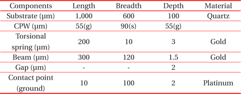
Switch specifications.
In spite of being a see-saw configuration, the proposed switch follows a different approach from former switches. The switch deflects only one side while it is in the OFF state at its rest position. This helps to eliminate the conventional problem of needing to provide actuation voltage twice, in both the ON and OFF states since the beam is closer to the ground. Hence, on the removal of the actuation voltage, the beam automatically moves up and makes contact with the ground. The switch design is simpler than the former designs, thus facilitating easy fabrication. Initially, pull up electrodes were not needed at the ground. However, they can be used when the stiction problem starts appearing due to the constant hitting of the beam over the contact area. Actuation applied to the electrode would render the signal line open, driving the switch to the up-state and relieving the beam of other mechanical disturbances in the presence of the actuation voltage. Thus, this would increase the life span and reliability of the switch.
(1) Up-state capacitance
Series capacitance (Cs) occurs between the t-line and the switch metal and the open ends of the t-line together constitute the parasitic capacitance (Cp). The up-state capacitance consists of series capacitance and parasitic capacitance. The total up-state capacitance of the series switch is the same as that of a capacitive switch and is given by

The series capacitance, Cs, is composed of two components: parallel-plate (Cpp =
(2) Current distribution
Since in down-state the series switch is simply a continuation of the t-line, the current distribution on a series switch in the down-state position is very similar to that of the coplanar wave-guide. Simulations have shown that irrespective of the width of the signal line, the edges of the bridge are the locations of the current concentration. Therefore, if small holes are placed in the centre of the bridge, the switching time will decrease (less air resistance) without affecting the current distribution.
(3) Down-state resistance
The down-state resistance of the MEMS switch is a result of contact between the cantilever and the signal line. A short section of the t-line together with the DC contact area builds down-state resistance. The mechanical force applied, the contact area and the quality of the metal-to-metal contact determine the contact resistance. The MEMS series switch resistance between the contact areas is dependent on its effective length and width. The total switch resistance for a series switch with one contact area is:

where Rs1 is the signal line loss, Rc is the resistance at the contacts and Rl is the resistance of the beam.
(4) Loss
Measuring the values of S-parameters or using a circuit simulator helps in the calculation of loss of a MEMS series switch. A CLR (capacitive inductive resistive) circuit can also be used for this calculation. Loss is independent of frequency.

The loss of the proposed switch is 0.2 dB.
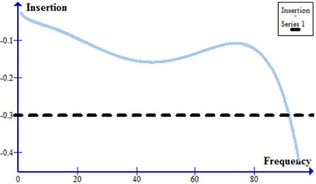
Owing to its design characteristics, the proposed switch, it provides excellent RF performance and requires low actuation voltage and traverse maximum bandwidth. All simulations were carried out in Ansoft HFSS. Upon actuation, the switch is driven into the ON state and provides an insertion loss of −0.02 dB .The switch has an insertion loss of as low as − 0.3 dB for a frequency span of 78 GHz. The insertion loss is shown in the Fig. 6.
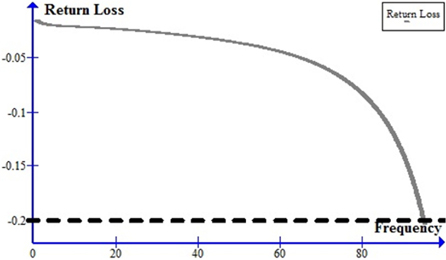
The return loss (shown in Fig. 7) is as low as − 0.02 dB indicating negligible power loss.
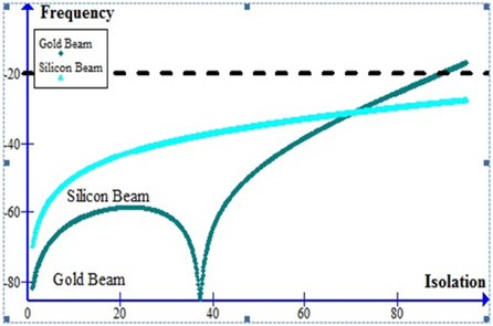
The advantage of the switch is that it remains in the OFF state when in the rest position. It also makes smooth contact with the ground thereby facilitating the isolation manifold. The isolation loss of the switch is as high as − 90.9 dB at 30 GHz and decreases to − 20.4 dB at 78 GHz. A variation in isolation loss is observed by using silicon as the see-saw beam as shown in Fig. 8.
From Fig. 8, it can be observed that silicon operates for a much wider bandwidth. It is found that silicon can be used as an alternative to the see-saw beam. This would reduce the spring constant and further lower the actuation voltage. Moreover, Au may fail to work at higher frequencies, while silicon gives satisfactory results, even at higher frequencies.
The see-saw beam eliminates any residual stress within itself and hence the spring constant does not contain a residual stress component. Due to its free state, the beam does not have a stretching component [2]. The spring constant of the beam is obtained by taking into account the assumption that the beam does not bend. Eq. (4) is the equation for the spring constant [12].

where

The spring constant of the beam is very low in comparison with the fixed-fixed beams with the same (
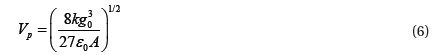
The dimensions of the switch given in Table 2 provide an actuation voltage of 5.46 V. The permittivity

where
The restoring force is the force required to retain the beam in its original position and is given by

where K is the spring constant of the beam and x is the gap between the signal line and the beam. The restoring force of the proposed beam is 0.4 μN which is as expected due to the see-saw structure.
The proposed see-saw switch is novel and yields the best RF performance obtained so far. The use of platinum contact points, the contact with the ground in up-state, the size of the switch and replacing the pivot boosts with the torsional spring have enhanced the reliability of the switch. The small size of the switch makes it faster between the two states. The good insertion loss, actuation voltage and high isolation verify the efficiency of the switch. The design is very basic and operates over the widest frequency so far seen for a see-saw type switch. This switch therefore has significant scope in many applications due to its wideband performance.