The active control of surface plasmon polaritons (SPPs), which empowers SPPs for the next generation photonic devices and circuits in terms of signal modulation and transmission, attracts considerable research enthusiasm especially in the last 15 years [1-3]. Both optically [4] and electrically [5] pumped gain media can be used for the active control of SPPs, whereas the latter is especially promising for high-density optoelectronic integration. In an active SPP device with electrically-pumped multiple quantum wells (MQWs) as the gain medium, the interface-bounded SPP mode requires MQWs in the modal field vicinity so as to maximize the modal gain [6]. Thus, the undoped separate confinement heterostructure (SCH) layer serving for carrier confinement has to be kept thin [7]. As such, the contact layer must be doped with low concentration in order to avoid diffusion of doped ions, which may spoil the high gain structure, into the MQWs. Since a heavily-doped contact cannot be allowed in such a case, the lightly-doped electric contact for active SPP devices needed to be investigated.
In this work, we investigated the fabrication of an
II. DEVICE STRUCTURE AND FABRICATION
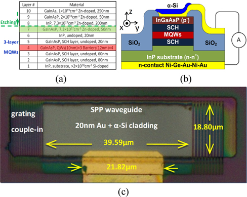
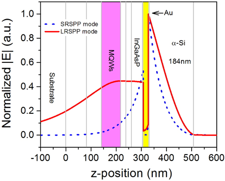
InP based wafers with 3-layer tensile strained InGaAsP MQWs are used as substrate, which provides optimized TM gain near telecom wavelength 1.55 μm for SPP propagation. As shown in Fig. 1(a), epitaxial layers above layer #7 were removed by highly selective chemical etching, leaving an atomic level smooth top surface. Considering the Si cladding could increase the coupling strength, the 50 nm p-doped InGaAsP layer was kept to improve electric contact, which allows us to avoid the trade-off between coupling strength and current injection efficiency to a certain degree. A mesa was etched through MQW’s depth with a sacrificial hard mask protecting the top surface, which was removed before Au film deposition as the SPP waveguide. After plasma etching, the sample was dipped into diluted HCl/HNO3 mixture. This non-selective etching helped to reduce the plasma damage from the mesa side wall. The mesa width is 20 μm and length is 60 μm. After electrical passivation and injection window opening, 2 nm Ni and 20 nm Au films were deposited on the mesa with waveguide strip and coupling grating defined by Electron Beam Lithography (EBL). Immediately after depositing Ni and Au, the samples were divided into four groups and annealed in an RTA furnace. The four groups of samples were all annealed with the temperature fixed at 400℃, and the duration time varying from 15s to 60s with 15s increment, respectively. After the RTA process, the metal film surface was studied with the scanning electron micrography (SEM) by means of the EBL technique. Finally, an amorphous silicon film was deposited on the top using an e-beam evaporator with slow rate for film quality and final thickness control. The silicon film was chosen as the dense cladding material because of its transparency in the near infrared (IR) region and the high refractive index to match that of the III-V semiconductor substrate. The α-Si thickness is ~184 nm. The schematic cross section of the fabricated device is shown in Fig. 1(b). The top view of the fabricated device is shown in Fig. 1(c). Here, the 184 nm-thick α-Si cladding plays a role in improving field intensity distribution in the gain region for the concerned SPP mode. Through the Transfer Matrix Method (TMM), the mode solving and analysis in the SPP waveguide were implemented. Two SPP modes, i.e. short-range SPP (SRSPP) and long-range SPP (LRSPP) are supported in the waveguide with the cladding thickness 184 nm. The effective modal indices of LRSPP and SRSPP are 3.24-0.0038i and 4.03-0.1234i, respectively. Figure 2 depicts the field spatial distribution of SPP modes. As shown in Fig. 2, the cladding improves the gain coupling factor for the LRSPP mode by increasing the SPP waveguide refractive index symmetry. On the contrary, the modal gain efficiency of the short-range SPP (SRSPP) mode is quite limited and rapidly diminishes during propagation.
III. EXPERIMENTAL MEASUREMENT AND ANALYSIS
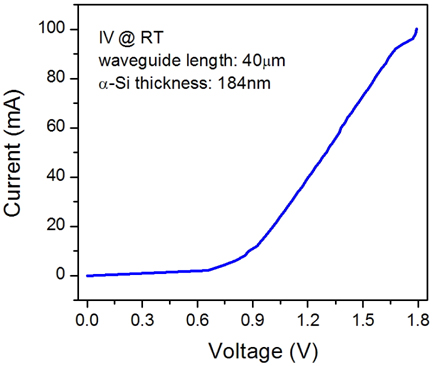
The device was tested with SPP excited by polarized laser with 1.55 μm wavelength through a 10× long working distance objective lens. The period of the input grating is 478 nm with 50% duty cycle for vertical coupling and the period of the output grating is 832 nm for decoupling into free space with off-axis angle 35°. Before the input coupling, a free space 1000 Hz chopper was inserted for modulating the input signal with constant frequency. Meanwhile, the device was biased by a high precision pulse current source with 1200 Hz frequency and 30% duty cycle. By analyzing the intensity of the decoupled light from the output grating into a multimode fiber probe, the lock-in amplifier was able to extract the signal referring to the differential frequency between the chopped laser and pulse current source. Extracted from the spontaneous emission and surface scattered light, the output signal directionally decoupled and collected from the measurement system based on the differential frequency reference approach was identified as the probe SPP signal amplified by stimulated emission [9, 10]. As shown in Fig. 3, the forward current-voltage (I-V) characteristic of the diode device was investigated at room temperature before the measurement to ensure that the electric device could work.
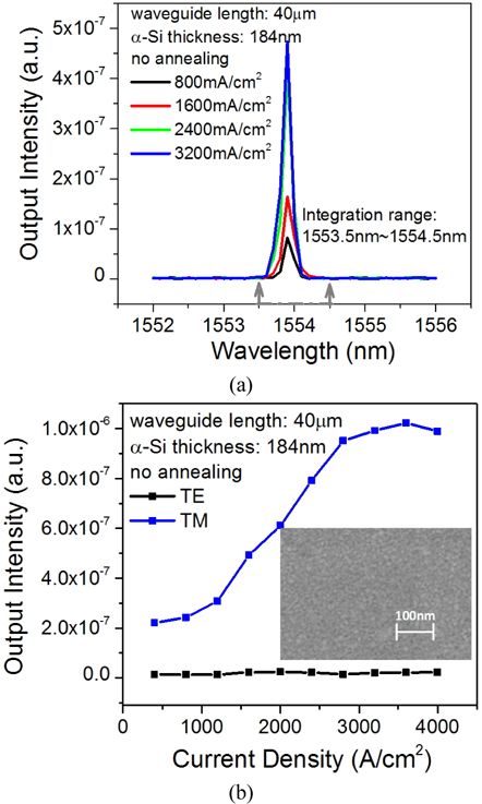
The output signal was analyzed using a high resolution monochromator, the output intensity was integrated near spectra peak ~1554 nm, and the integral range was located in 1553.5~1554.5 nm. In order to guarantee the spectra resolution, the monochromator slits were calibrated carefully and the scanning step was set as 0.1 nm. The measurement was repeated and the averaged data were derived for alleviating the random noise. Figure 4(a) shows that the spike intensity of the output signal rises with the increasing current density, which can be calculated with biased current intensity divided by the mesa area, the length of which is 20 μm over corresponding length of the metal waveguide. This sensitive response of the output signal intensity to the current density level tells that the stimulated emission from the MQWs has effectively coupled to the SPPs. By rotating the inline polarizer, the input signal with different polarization, i.e. the TE or TM mode, was respectively coupled into the planar waveguide to analyze their properties of propagation and gain modulation. The integrated output intensity measured on the sample device without annealing process for a different polarization mode was plotted as the function of the current density in Fig. 4(b). It is found that the TE mode signal was neither detected nor modulated by the electrical pumping, which proves that the collected signal is an SPP-related electromagnetic mode. This is because SPPs exist only for TM polarization, and no surface modes exist for TE polarization in metal-dielectric multilayer planar waveguide systems [11].
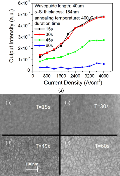
The influence of RTA temperature was firstly investigated by observing the contact surface morphology of Ni-Au and bulk material. It was found that, at the same annealing time, the surface morphology was hardly changed before the RTA temperature exceeded 400℃, while lots of clusters began to appear on the contact surface over 400℃. Hence, the annealing temperature was fixed at 400℃ in the annealing treatment of devices for the following measurement. The measurement was conducted on the four groups of samples with different RTA duration times. In Fig. 5(a), the output intensity of SPP signal with electrical compensation under different injection current levels derived from the abovementioned approach is plotted as a function of the current intensity. The output intensity of SPPs was observably enhanced with the improvement of injected current density before the duration time exceeded 30s. However, compared to the case of the sample without annealing in Fig. 4(b), it can be found that the output intensity has become weaker under the same current injection. Longer annealing time (45s) would drastically decrease the SPP output signal intensity even under sufficient current injection. It seems that the annealing process has notably impaired the SPP propagation and its loss compensation by electrical pumping. When the duration approaches 60s, the SPP propagation is almost not supported by the waveguide device any more. In order to intuitively illustrate these results, the surface morphology SEM images of the metal film within the waveguide strip region after different RTA treatments are scanned and shown in Fig. 5(b)~(e). It can be found that the surfaces obtained after annealing 15s and 30s are relatively smooth. The surface roughness significantly increased when the duration approached 45s. When the duration time approaches 60s, the morphology of contact surface is changed so severely that the SPPs could no longer propagate on it. It seems that eutectic mixture significantly increases the surface roughness of the thin metal film (2 nm Ni and 20 nm Au). If a heavily-doped ohmic contact for an active SPP device cannot be obtained, the metal-semiconductor Schottky contact can be an alternate solution [7]. Moreover, double-metallic waveguide layer can be adopted to enhance the Purcell effect in the radiative recombination related device [12].
In summary, we have studied the influence that RTA treatment exerts to Au/Ni-based electric contact formed on the lightly doped III-V semiconductor surface for active control of SPPs propagation. It is found that the RTA process would change the thin metal film (2 nm Ni and 20 nm Au) morphology, lead to the restriction of SPP propagation, and eliminate the positive role played by the RTA in metal-semiconductor electric contact optimization. With the increase of annealing duration time, more significant degradation of the electrical-pumping compensation for SPP propagation loss generates even under sufficient current injection when the annealing temperature is fixed at 400℃. Long annealing duration time (60s) will increase the SPP waveguide interface roughness so severely that the SPP signal nearly can no longer propagate on it. This study would be of valuable reference to the circumstance of lightly-doped electric contact for SPP waveguide devices when heavily-doped contact cannot be obtained.