III-nitride compounds have attracted considerable interest in the last decade due to their wide application in solid-state-lighting devices, which are used widely in the blue/green and ultraviolet spectral regions with higher quantum efficiency [1-3]. AlGaN alloys are important for optoelectronic devices such as light-emitting diodes (LEDs), laser diodes (LDs) and photo-detectors in the UV spectral region between the wavelength range from 200 nm to 365 nm, which can be tuned according to Al content in the AlGaN alloy system [4]. Owing to difficulty in fabricating bulk GaN and AlN, nearly all AlGaN films are heteroepitaxially grown on lattice-mismatched substrates, such as sapphire and SiC substrates, which results in threading dislocations, and residual strains occur greatly in AlGaN epifilms. For reducing the threading dislocation density, a thin AlN nucleation layer or GaN buffer layer is utilized to improve the crystal quality [5-7]. D H Wang
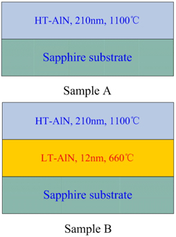
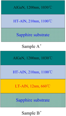
Growth of an HT-AlN nucleation layer was achieved using a cold-wall showerhead low-pressure metal-organic chemical vapor deposition (LP-MOCVD) system. Hydrogen was used as carrier gas, triethylaluminum (TEAl), triethylgallium (TEGa) and ammonia (NH3) were used as Al, Ga and N sources, respectively. The pressure of the LP-MOCVD growth system was about 5.2×10⁻³ Torr, and the calculated ratio of V/III (NH3/TEAl) is 7058. As shown in Fig. 1, a 210-nm-thick HT-AlN nucleation layer was first deposited on (0001) sapphire substrate (2 inch) at 1100℃ denoted as Sample A. Sample B has the same structure except that a 12-nm-thick LT-AlN nucleation layer was grown at 660℃ between the sapphire substrate (2 inch) and a 210-nm-thick HT-AlN nucleation layer. In order to study and analyze the influence of the LT-AlN nucleation layer on AlGaN epifilms, we have grown an AlGaN with 1200-nm-thickness on Sample A and Sample B at 1030℃. The as-grown samples were characterized by high resolution X-ray diffraction (HRXRD), atomic force microscopy (AFM), scanning electron microscope (SEM) and Raman scattering. For the purpose to reveal and obtain a comprehensive knowledge of the threading dislocation density of AlGaN epifilms grown on the two AlN nucleation layers, we measured X-ray rocking curves (XRCs) for both symmetry and asymmetry diffraction planes by HRXRD. The HRXRD was performed using Bruker D8-discover system equipped with Ge (220) monochromator and channel-cut analyzer, delivering a pure Cu-K
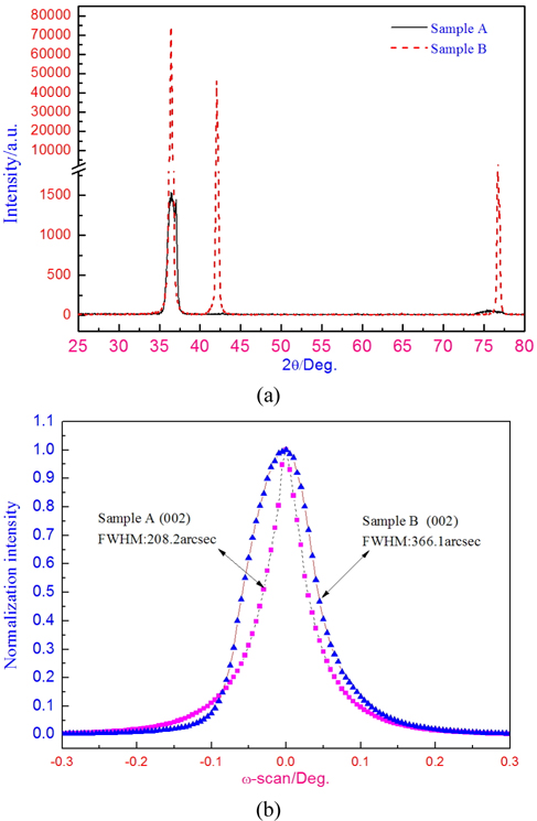
3.1. High-resolution X-ray Diffraction
XRD-2
3.2. AFM, SEM and Surface Morphology
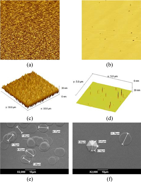
Figure 3 shows the 10×10 μm2 AFM images of the two HT-AlN nucleation layers. We can see the differences in surface morphology between Sample A and Sample B. The micrograph in Fig. 3(a) and (b) indicates an improvement of quality of HT-AlN nucleation layers. These V-shaped pits are similar to those observed in c-plane GaN epifilm. It was found that the number of V-shaped pit defects on the surface of Sample B is less than on Sample A when a thin film LT-AlN nucleation layer is grown on sapphire substrates. Figs. 3(c) and (d) show the 3D surface morphology of the two HT-AlN nucleation layer samples. It is seen that Sample B shows clearly a lower quantity of dislocations on the surface than Sample A does. In addition, the root mean square (RMS) value is 4.09 nm for Sample A and 0.47 nm for Sample B, which indicates that Sample B has a smoother surface morphology than Sample A does. Furthermore, we have carried out SEM analysis in Figs. 3(e) and (f). As can be shown, there appear irregular convex disks on the surface of Sample A and regular convex disks on the surface of Sample B. From a quantitative point of view, the number of irregular convex disks for Sample A is more than Sample B has. We have marked the size of convex disks, and found the size of the convex disks on Sample A is a little smaller than those on Sample B. Consequently, be that as it may, the higher crystal quality of HT-AlN nucleation layers can be obtained by insertion of the LT-AlN nucleation layer between the sapphire substrate and the HT-AlN nucleation layer.
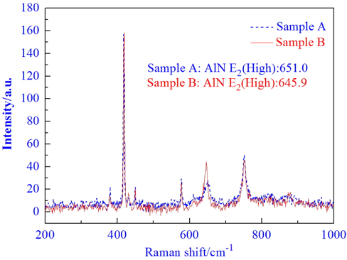
Raman scattering was performed to examine residual strain of the two AlN nucleation layer samples recorded in the z(xx)-z backscattering configuration with 514-nm wavelength at room temperature. As is well known, the lattice and thermal mismatch between the substrate and the epifilm, characteristic for the heteroepitaxial growth of nitrides on a foreign substrate, results in the presence of strain under a linear elasticity biaxial system [11, 12]. Phonon frequency shifts are often employed as a tool for strain assessment in mismatched semiconductor heterostructures. The Raman scattering spectra of Sample A and Sample B are shown in Fig. 4 for a comparison. As can be shown in Fig. 4, the Raman peaks located at 651.0 cm−1 and 645.90 cm−1 are E2 (high) phonon modes for Sample A and Sample B, respectively. It was well known that the red-shift of AlN E2 (high) phonon mode corresponds to tensile strain in the HT-AlN nucleation layer, which is caused by differences in the thermal expansion coefficient and lattice mismatch between the AlN epilayer and sapphire substrate [5, 9]. The theoretical value of E2 (high) for AlN is 657.4cm−1 of stress-free [13, 14], so there existed red-shift of AlN E2 (high) mode of 6.4 cm−1 and 11.5 cm-1 relative to the theoretical value of 657.4 cm−1 for Sample A and Sample B, respectively, which implies that Sample A and Sample B are under tensile strain, and the tensile strain existing in Sample B is larger than that in Sample A. As we know, the strain along the growth direction is found to be tensile as elasticity theory predicts in the case of biaxial stress [15-18]. By comparison to the number of V-shaped pits, more tensile strain can be relieved in the condition of more V-shaped pits on the surface of Sample B. Furthermore, it is widely accepted that the larger tensile strain existing in-plane is apt to produce high crystalline quality epifilm. Thus, the conclusion can be drawn that inserting the LT-AlN nucleation layer can improve crystal quality of the HT-AlN nucleation layer.
In order to study further the influence on the crystal quality for AlGaN epifilms by inserting the LT-AlN nucleation layer, we grew an AlGaN with 1200-nm-thickness on Sample A and Sample B at 1030℃, as denoted as Sample A’ and Sample B’ respectively, as shown in Fig. 5. In Ref.[9], we have carried out the symmetrical (002) and asymmetrical (102) XRD-
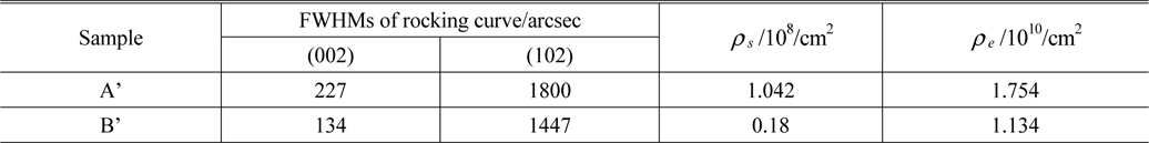
FWHMs and the calculated threading dislocation densities of AlGaN epifilms on Sample A’ and Sample B’
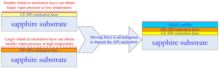
Ref. [19] studied the size of AlN island under different growth temperature modes, as can be seen from Fig. 6, the size of AlN islands grown under low-temperature mode is smaller than the size of those grown under intermediate temperature and high temperature [19], which coincides with AFM images results.
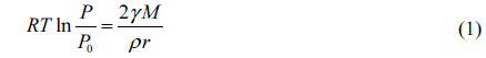
It was well known that the relationship between saturated vapor pressure and radius of grain in a nucleation layer is shown as the Kelvin formula in Eq. (1):

Here,
In this paper, we have focused on the influence on AlN nucleation layer and AlGaN layer caused by inserting a LT-AlN nucleation layer between the c-plane sapphire substrate and HT-AlN nucleation layers. HRXRD, AFM, SEM and Raman scattering have been employed to characterize crystal quality, surface morphology and residual strain of HT-AlN nucleation layer and AlGaN epilayer. Results indicated that crystal quality of HT-AlN and AlGaN layer can be improved greatly, and the threading dislocation density existing in AlGaN epifilms has been reduced when LT-AlN nucleation layer was inserted, which is consistent with the surface morphology of the HT-AlN nucleation layer and AlGaN epifilm probed by AFM and SEM.