Three-dimensional (3D) integrated-circuits (ICs) have better performance and energy efficiency, and a smaller footprint in electronic systems than two-dimensional (2D) ICs because of their smaller form factor due to 3D stacking and 3D interconnections [1]. Compared with the currently available through-silicon via (TSV)-based 3D ICs [2], the monolithic 3D IC (M3IC) [3-12], in which each circuit layer is thin and is fabricated directly over the previous circuit layers on the same substrate, is a promising technology that enables ultrafine-grained vertical integration of devices and interconnections with the conventional monolithic inter-tier vias (MIVs) to connect the various layers.
There have been extensive studies of process, device, and circuit technologies for the M3IC [3-12]. SRAM and inverters utilizing dynamic threshold voltage (VTH) modification thanks to the electrical coupling between stacked top and bottom metal-oxide-semiconductor field-effect transistors (MOSFETs) have been demonstrated when the inter-layer dielectric (ILD) is very thin (tens of nanometers) [12]. However, to our knowledge, no studies have been published that evaluate a regime in which the electrical coupling between the stacked FETs is either considered or not. Therefore, to design and analyze M3ICs precisely with an ultra-thin ILD, regimes in which the electrical coupling between the stacked FETs is included must be systematically investigated.
In this paper, the electrical coupling between the stacked top/bottom FETs in two types of monolithic 3D inverter (M3INV), of which one includes a metal layer (ML) in the bottom tier and the other does not include a ML, will be systematically investigated using a 3D device simulator. Device characteristics of the two types of M3INV will be surveyed in terms of electrical coupling between the stacked top/bottom FETs (Section II). Next, the regime of the sizes and materials of the ILD, as well as the doping concentration and length of channel where the stacked FETs are coupled will be studied (Section III). Finally, Section IV will conclude this paper.
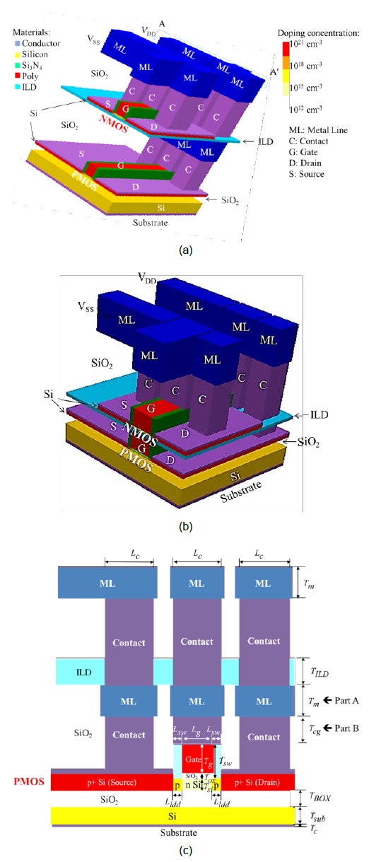
Fig. 1 shows the schematics of two examples of types of M3INV structure. Fig. 1(a) and (b) show Structure A [9,10], which includes the MLs between the top and bottom tiers and Structure B [3,6], which excludes them, respectively. Fig. 1(c) shows the cross-section of A-A′ in Structure A shown in Fig. 1(a). The cross-section of A-A′ in Structure B is the same as that shown in Fig. 1(c) except that MLs (Part A) and contacts (Part B) would be added. Here Lg, Lsw, Lldd, Lc, Tg, Tox, Tsi, Tsw, TBOX, Tsub, Tc, TILD, Tcg, and Tm denote gate length, sidewall length, lightly-doped drain length, contact length, gate thickness, gate-oxide thickness, silicon-channel thickness, side-wall thickness, buried-oxide thickness, silicon-substrate thickness, contact thickness, ILD thickness, bottom-gate contact thickness, and ML thickness, respectively. To compensate for the hole/electron mobility skew, the width of the PMOSFET is larger than that of the corresponding NMOSFET. To increase the cell footprint by allowing for extra space for MIVs (or contacts) connecting the top and bottom tiers, the PMOSFET and NMOSFET are placed on the bottom and top tiers, respectively [9]. Each MOSFET consists of a source (S)/drain (D) highly doped with 1021 cm-3 and lightly-doped with 1018 cm-3, the gate-oxide (SiO2), and the polysilicon gate (G). Lsw, Lldd, Lc, TBOX, Tsub, Tc, Tcg, and Tm are fixed as 10, 10, 50, 30, 50, 6, 100, and 100 nm, respectively. According to the technology roadmap of the fully-depleted silicon-on-insulator (FDSOI) [1,13], Lg (≈ Tg), Tox, Tsi, and Tsw (=Tg+Tox) are varied, and TILD is also varied to investigate the coupling effect.
[Fig. 1.] Schematics of two types of monolithic 3D inverter cells. (a) 3D schematic of Structure A with a metal layer in the bottom tier, (b) 3D schematic of Structure B without the metal layer, and (c) cross-section of A-A′ in Structure A shown in Fig. 1(a). ML, C, G, D, and S denote the metal layer, contact, gate, drain, and source, respectively. Materials in the structure and doping concentration in the silicon body are denoted by color.
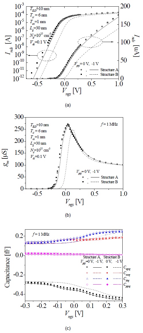
Fig. 2 shows the DC/AC coupling between the bottom and top MOSFETs with Lg = 30 nm, Tsi = 6 nm, and Tox = 1 nm [13] in the M3INV cells with the ultra-thin ILD (TILD = 10 nm), using the 3D technology computer-aided design (TCAD) numerical simulator, ATLAS [14]. Fig. 2(a), (b), and (c) show the drain-source current (Inds), trans-conductance (gm = dInds/dVngs), and capacitances (Cngng, Cnsng, Cdng, Cpgng) versus the top-gate voltage Vngs of the top NMOSFET at different bottom-gate voltages Vpgs’s (0 and –1 V), respectively. The drains in both the bottom and top MOSFETs are common and can be operated as the output. The sources and gates in the bottom and top MOSFETs are grounded and separated, respectively. The drain-source voltage Vds is biased as 0.1 V. In Fig. 1(b) and (c), frequency f = 1 MHz is applied for AC characterization. The electrical coupling of the bottom PMOSFET due to the gate of the top NMOSFET can be ignored [11].
[Fig. 2.] (a) Inds-Vngs characteristics (linear and logarithmic), (b) transconductance (gm = dInds/dVngs), and (c) capacitance (Cngng, Cnsng, Cdng, Cpgng) of the top transistor in the M3INV cells (Structure A and B) as shown in Fig. 1(a) and (b). Symbols and lines denote Vpgs = 0 and -1 V, respectively. Empty and filled symbols denote Structure A and B, respectively. Here, Lg = 30 nm, TSi = 6 nm, Tox = 1 nm, TILD = 10 nm, Nd (Na) = 1015 cm-3, and Vds = 0.1 V. f = 1 MHz is applied for AC characterization. The subscripts nds, ngs, pgs, ngng, nsng, dng, and pgng denote drain-to-source of the NMOSFET, gate-to-source of the NMOSFET, gate-to-source of the PMOSFET, gate-to-gate of the NMOSFET, source-to-gate of the NMOSFET, drain-to-gate of the NMOSFET, gate of the PMOSFET-to-gate of the NMOSFET, respectively.
In this paper, the electrical coupling of the top NMOSFET will be quantified when the gate of the bottom PMOSFET is biased as two different voltages (0 and –1 V).
Empty and filled symbols denote Structure A and B, respectively, and symbols and lines denote Vpgs = 0 and –1 V, respectively. Inds–Vngs, gm, Cngng, Cnsng, Cdng, and Cpgng of the top NMOSFET in Structure A and B have small and large differences between Vpgs = 0 and –1 V, respectively. As shown in Fig. 2, the electrical coupling can be ignored when the distance between the channel of the top NMOSFET and the gate of the bottom PMOSFET is over 100 nm (e.g., 210 nm at Structure A) and the electrical coupling should be considered when it is below 100 nm (e.g., 10 nm at Structure B).
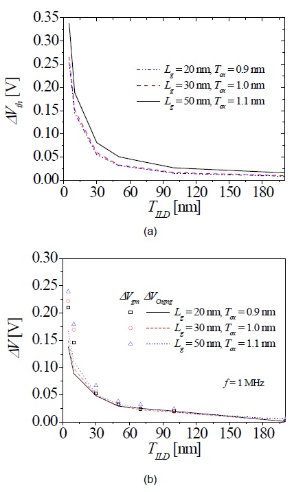
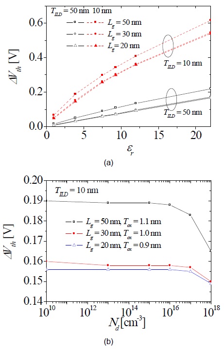
Under what geometry or process conditions may the electrical coupling between the bottom and top MOSFETs be neglected? In order to investigate the coupling effect in three types of Structure B, the threshold voltage shift (ΔVth), the voltage shifts of transconductance gm (ΔVgm), and the top gate-to-top gate capacitance Cngng (ΔVCngng) for electrical coupling were systematically quantified for various values of TILD, the dielectric constant εr of ILD, while the doping concentrations Nd (or Na) in the channel were simulated with the 3D TCAD numerical simulator, as shown in Figs. 3 and 4. Threshold voltage Vth is defined as Vngs when Inds = 10-7 A. ΔVth, ΔVgm, and ΔVCngng are defined as the differences between Vths and Vngss at the maximum gm, and Vngss at maximum dCngng/dVngs of the top NMOSFET between Vpgs = 0 and –1 V, respectively. Among three types of Structure B, one is Lg = 50 nm, Tsi = 10 nm, and Tox = 1.1 nm, another is Lg = 30 nm, Tsi = 6 nm, and Tox = 1 nm, and the third is Lg = 20 nm, Tsi = 6 nm, and Tox = 0.9 nm, which follows the FDSOI technology roadmap guideline [1,12]. Fig. 3(a) and (b) show ΔVth and ΔVgm (or ΔVCngng) versus TILD, respectively. When TILD values are over 50 nm, ΔVth, ΔVgm, and ΔVCngng are below 50 mV, and thus the coupling in the structures can be ignored. However, when TILD values are below 50 nm, the coupling must be considered.
Figs. 4(a) and (b) show ΔVth versus the dielectric constant εr of the ILD and ΔVth versus the doping concentration Nd (or Na) in the channel, respectively.
In Fig. 4(a), as εr increases, ΔVth increases in all of three types of Structure B. In Fig. 4(b), as the doping concentration increases to over 1016 cm-3, ΔVths decreases in all three types of Structure B. Likewise, at all doping concentrations in the channel below 1016 cm-3, ΔVths is almost constant in all of the three types of Structure B.
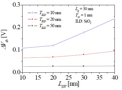
Fig. 5 shows ΔVths versus the side-wall length LSW of the top transistor in the M3INV cell at different TILDs. As the TILD decreases, ΔVth increases in all regimes of LSW in all of three types of Structure B, and in all regimes of LSW below 20 nm, the ΔVths are almost constant in all of the three types of Structure B.
When TILD ≥ 50 nm and εr ≤ 3.9 in Structure B, the interaction between the stacked MOSFETs can be neglected, but for one with an ILD thickness or material that does not fit the above conditions, the interaction must be considered.
In this paper, we investigated the electrical coupling between the stacked top/bottom FETs in the M3INV. To investigate the coupling between the stacked devices, the drain-source currents versus the gate voltage of the bottom FET in the M3INV were simulated using a 3D device simulator with varying channel length, thickness of the ILD, material of the ILD, doping concentration in the channel, and side-wall length. When the doping concentration was below 1016 cm-3 and the side-wall length was below 20 nm, the threshold voltage shifts are almost constant in all of the three types of Structure B. The interaction between the stacked MOSFETs can be neglected in the M3INV with TILD ≥ 50 nm and εr ≤ 3.9, but the interaction must be taken into account with ILD thicknesses and materials with other values. Thus a new method for accurate simulation in conventional circuit simulators may be required for circuits consisting of coupled devices.