Indium tin oxide (ITO) films deposited on glass substrates have been widely used as a transparent conducting electrode for its applications in devices such as solar cells, touch panels, organic light-emitting diodes, and liquid crystal display (LCD) s due to their visible transparency (~90%) and low resistivity (2−4×10⁻⁴ Ω/cm) [1-9]. However, undesirable damage to the opto-electronic device may be caused during deposition of ITO films by direct current (DC) or radio frequency (RF) sputtering [10]. In addition, the easy formation and propagation of cracks in the brittle ITO film have been critical drawbacks [11,12]. For these reasons, some thin transparent conducting film (TCF) materials such as metal nanowire networks, conducting polymers, carbon nanotubes, graphene, and several conducting oxides have been suggested as promising alternatives to ITO films [13-21]. Other promising candidates for the ITO film are oxide-metal-oxide (OMO) multilayer films, viewed to be advantageous due to their low sheet resistance, high transparency, and flexibility. Although good electrical and optical properties of OMO multilayer films including IZO/Ag/IZO, ITO/Ag/ITO, IZTO/Ag/IZTO, AZO/Ag/AZO, GZO/Ag/GZO, NTO/Ag/NTO, and ZTO/Ag/ZTO schemes have been reported [12,22-27], further investigation of OMO materials remain. Specifically, Ni-doped indium zinc oxide (NIZO) is regarded as a promising candidate of TCF because transparent conductive NiOx components induce the enhancement of electrical and optical properties of IZO films.
In this work, we demonstrated LCDs utilizing NIZO and NIZO/Ag/NIZO multilayer films as a substitute for ITO electrodes. Electrical properties of NIZO and NIZO/Ag/NIZO multilayer electrodes were measured. Electro-optical (EO) properties of twisted nematic (TN) liquid crystal (LC) cells also measured to confirm the potential of the NIZO and NIZO/Ag/NIZO multilayer films to be applied as the transparent conducting electrodes of LCD applications.
Prior to the deposition of NIZO and NIZO/Ag/NIZO multilayer films, the glass substrates were cleaned by ultrasonication in acetone, isopropyl alcohol, and DI water for 10 min each, and were then dried with N2 gas. RF/DC magnetron sputtering system (SELCOS-01) was used to uniformly deposit the NIZO and NIZO/Ag/NIZO multilayer films. The used NIZO target (99.9%, 8 in.) was composed of NiO, ZnO, and In2O3 with 10.5 mol%, 15.7 mol%, and 73.8 mol%, respectively. During the deposition of the NIZO film, the sputtering conditions were maintained constant at a working pressure of 0.33 Pa, an RF power of 300 W, and an Ar flow rate of 90 sccm, respectively. The substrate-to-target distance was 150 mm perpendicularly and the substrate holder was rotated during the sputtering. Subsequently, an Ag layer was selectively deposited on the bottom NIZO layer by DC magnetron sputtering using an Ag target (99.99%, 8 in.). The deposition conditions of the Ag layer were the same as that of the NIZO film, except for the DC power of 200 W. The sheet resistance and transmittance of NIZO and NIZO/Ag/NIZO multilayer films were measured by using a four-point probe system and by utilizing a UV-VIS-NIR spectrometer (V-650, JASCO Co.). Commercially available ITO coated glass substrates were used as a comparison. The NIZO and NIZO/Ag/NIZO multilayer films were characterized by field-emission scanning electron microscopy (FE-SEM; S-4200, Hitachi). A 50-nm-thick homogeneous polyimide (PI) was uniformly coated by means of a spin-coating method onto NIZO and NIZO/Ag/NIZO multilayer electrodes to form LC alignment layers; the PI was prebaked at 80℃ and then imidized at 230℃ for 1 hr. To achieve homogeneous LC alignment, the PI layer was rubbed by using a unidirectional rubbing method. The rubbing strength was conventionally optimized and set at 300 mm. TN cells were fabricated to allow measurement of EO characteristics in cell gaps of 5 μm. Commercial positive LCs (Δε=10.7, no=1.4756, ne=1.5702, Merck) were injected into each cell at room temperature by means of capillary force. We confirmed LC alignment characteristics by using a photomicroscope (BXP 51, Olympus). The EO characteristics of rubbing-aligned TN cells were measured by using an LCD evaluation system (LCMS-200, Sesim Photonics Technology).
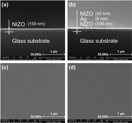
Figure 1 shows the FE-SEM images of 150-nm-thick NIZO and NIZO/Ag/NIZO multilayer films. Figures 1(a) and 1(b) show cross-sectional FE-SEM images of single NIZO and NIZO/Ag/NIZO multilayer films. While the thickness of single NIZO film was set at 150 nm, the thicknesses of NIZO/Ag/NIZO were set at 42 nm, 8 nm, and 100 nm, respectively. To facilitate direct comparison with NIZO and NIZO/Ag/NIZO multilayer films, we deposited at approximately the same thickness. The surficial FE-SEM images of NIZO and NIZO/Ag/NIZO multilayer films show that their surfaces are smooth and uniform irrespective with base layers as shown in Figs. 1(c) and 1(d).
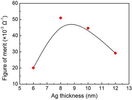
To determine the optimized thickness of the Ag layer in the NIZO/Ag/NIZO multilayer film, a figure of merit (
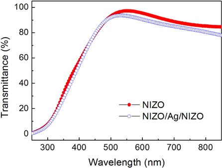
The electrical sheet resistances of NIZO and NIZO/Ag (8 nm)/NIZO (hereinafter denoted as NIZO/Ag/NIZO) multilayer films were found to be 46.84 Ω/□ and 9.87 Ω/□, respectively. The multilayer film showed a much lower electrical sheet resistance. On the contrary, NIZO/Ag/NIZO multilayer films showed a lower optical transmittance (93.36%) at a wavelength of 550 nm compared to the single NIZO film (97.28%) as shown in Fig. 3.
Calculated
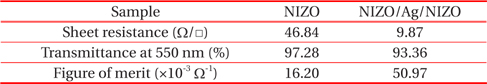
Comparison of the electrical sheet resistance, optical transmittance, and figure of merit value of NIZO and NIZO/Ag/NIZO multilayer films.
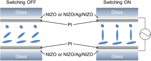
The EO characteristics of the TN cells were investigated to examine the potential application of NIZO and NIZO/Ag/NIZO multilayer films as a transparent conducting electrode in LCDs.
Figure 4 shows the schematic diagrams of the TN cell and its operation. When an appropriate voltage is applied between the NIZO or NIZO/Ag/NIZO electrodes, the LC molecules are homeotropically reoriented. The waveguide effect caused by LC molecular reorientation can enable the incident light to pass through the LC cells.
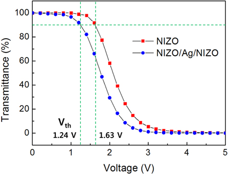
The performance of the TN cell is related to the movement of LC molecules according to voltage switching, which is determined by measuring the EO characteristic of voltage-transmittance (V-T). V-T curves were acquired for TN cells fabricated based on NIZO/PI and on NIZO/Ag/NIZO/PI electrodes. The threshold voltage (Vth)s of the NIZO/PI and on NIZO/Ag/NIZO/PI electrode TN cells at a transmittance of 90% were 1.63 V and 1.24 V, respectively, as shown in Fig. 5.
This result demonstrates that the use of the NIZO/Ag/NIZO electrode enhanced the V-T characteristics of the TN cell. We attributed this phenomenon to the electric field enhancement effect, given that multilayer electrode can easily induce electric field due to low sheet resistance. In the NIZO/Ag/NIZO electrode, when the stronger electric field was exposed to an alternating voltage, it polarized the LC molecules at a low voltage. Low operation voltage can be achieved by using the NIZO/Ag/NIZO electrode, which is an important factor in LCD power consumption.
In addition, The Vth of the TN cell for the NIZO/Ag/NIZO multilayer electrode was similar to the TN cell for the conventional ITO electrode (1.2 V) reported in Ref. [29].
In conclusion, NIZO and NIZO/Ag/NIZO multilayer films were examined for application as transparent electrodes in LCDs. The NIZO and NIZO/Ag/NIZO electrodes were uniformly deposited using DC and RF sputtering. When the Ag layer was interposed between the NIZO layers, the loss of optical transmittance occurred. However, the Ag layer brought enhancement of electrical sheet resistance to the NIZO/Ag/NIZO electrode. The NIZO/Ag/NIZO electrode with 8-nm-thick Ag layer exhibited an outstanding figure of merit value, which is similar to the conventional ITO electrode. In addition, the potential of the NIZO and NIZO/Ag/NIZO multilayer films for use in LCD electrodes was confirmed. The TN cell based on the NIZO/Ag/NIZO electrode exhibited superior EO characteristics than that based on the single NIZO electrode, which was competitive compared to those based on a conventional ITO electrode. Therefore, the NIZO/Ag/NIZO multilayer film has excellent potential as a transparent electrode in LCDs, potentially substituting the conventional ITO.