A photocathode emits electrons when it is exposed to light. When it absorbs light, electrons in the valence band are transported into the conduction band. A portion of the absorbed light is responsible for the electron transport. Of these transported electrons, a subset diffuse to the cathode surface directly without suffering collisions with the lattice. Some of these electrons have sufficient kinetic energy to overcome the barrier due to electron affinity and contribute to direct photoemission. The three successive step model - optical absorption, electron transport, and escape across the surface - has provided a useful description of the process of photoemission for both fundamental and practical applications [1]. Thus, photoemission is a process in which photons are converted into free electrons.
The traditional method of photocathode manufacturing is complicated and complex. It requires ultra-high vacuum (UHV) conditions with at least 10−7 torr during the manufacturing processes [2,3,4-7]. In addition, it requires specialized and expensive equipment. Moreover, it can only be performed by highly trained engineers. The photocathode formation area is usually small. Thus, it is limited to small-sized and highly specialized device applications.
Technology development in atmospheric manufacturing methods, including a new low temperature hermetic sealing techniques, creates a core technology foundation and path for low cost photocathode formation. This enables the integration of the low cost photocathode into a variety of current, new, and future applications in the form of traditional electronic devices such as optical devices, electron sources, and electron beam lithography to advanced devices such as medical imaging instruments.
Cs3Sb, a well-known mono-alkali photocathode from the photomultiplier tube industry, has many advantages for electronic device applications [1,8]. It is intrinsically a p type semiconductor, having a reflective emission mode with a long electron diffusion length and high quantum efficiency (QE) in the visible spectral range. Unlike negative electron affinity materials, which owe their high QE essentially to a monolayer of Cs adsorbed at the surface, Cs3Sb photocathodes are bulk materials in highly crystalline form and thereby posses a superior lifetime as desired in the accelerator environment. It is simpler to manufacture than the multi-alkali photocathode such Cs2KSb or Na2KSb, yet has a good response in the visible spectral range. In addition, it can be easily converted from the p type semiconductor to an n type semiconductor by adjusting the amount of Cs in the thermo-chemical Cs-Sb reactions.
In the present study, we introduce a new concept for a planar light source utilizing Cs3Sb photocathodes as flat electron emitters, which is viable for low-cost manufacturing and suitable for general applications. Among the numerous applications, we primarily consider here a flat-panel type lighting device that is mercury-free and has a high-efficiency cathodoluminescent light source that uses a cesium antimonide photocathode as a source of electrons and a layer of industrial P-22 phosphor as a source of light of desirable color wavelengths. By observing a variety of optical parameters, we examine the light emission characteristics of the planar lighting devices with the Cs3Sb photocathode emitter. We find that the cesium antimonide planar light source in a simple diode structure has bright, uniform and stable light emission characteristics without fluctuation over time. It also demonstrates the possibility of low power consumption to produce a more directable and easily controllable stream of electrons. These make it suitable for a variety of flat-panel lighting device applications.
UHV conditions are generally required to form photocathodes. There is no exception in this case. However, we have developed a process of fabricating Cs3Sb photocathode under atmospheric conditions. The Cs3Sb photocathode was formed by newly developed process technology and successive in-situ device fabrication, which was carried out in a process chamber. Performance testing of the Cs3Sb photocathode vacuum device was followed.
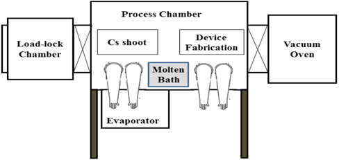
Figure 1 shows an experimental set-up for the formation of the Cs3Sb photocathode and device fabrication. It is connected with a load-lock chamber and a vacuum oven on the sides and a thermal evaporator at the bottom. The vacuum oven is for the thermal treatment of device components. The thermal evaporator deposits Sb film on the metal layer for the device.
The chamber is filled with an inert gas, such as Ar or N2, in order to prevent reaction between the reactive Cs3Sb photocathode and O2 or H2O molecules. There is a molten bath inside the chamber. It is filled with Na metal. Na metal is very reactive and acts as a getter, absorbing O2 and H2O molecules. Thus, O2 and H2O levels in the chamber are maintained below 0.01 ppm, respectively, in a strictly controlled manner.
For the formation of the Cs3Sb photocathode, we prepared a microstructure of a metal sheet with patterned micro-holes. The microstructure should be conductive.
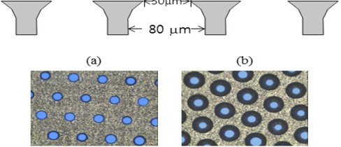
Figure 2 represents a clean microstructure with patterned micro-holes, showing schematic images of the top and bottom surfaces. The thickness of the microstructure is 100 μm. A diameter of a hole on the top surface is 30 μm while that on the bottom surface is 80 μm. The difference in diameter of the holes was caused by the anisotropic characteristics of wet etching.
Thin Sb film was deposited on the bottom surface of the clean microstructure by thermal evaporation. The thickness was 300 Å. A mask with a 2-inch diameter hole was attached on the Sb surface for Cs deposition. Subsequently, Cs shooting deposition was carried out on the Sb film surface with the mask. Upon Cs evaporation, Cs reacts with Sb thermo-chemically to yield Cs3Sb. This reaction occurs immediately to form the intrinsic p type crystalline Cs3Sb photocathode. The thickness was controlled by the evaporation time. The Cs evaporation time was less than 20 seconds. With excessive evaporation time, p type Cs3Sb photocathode is converted to p type with excessive Cs amount. Both p type and n type Cs3Sb photocathodes exhibit crystalline materials and the reflection mode of photoelectron emission. This microstructure with photocathode formed on the bottom side was attached on the cathode plate for device fabrication. In addition, in-situ device fabrication was followed in the process chamber.
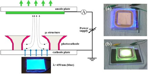
For device fabrication, we prepared the following device components: an anode plate with phosphor, a frame, a cathode plate with microstructure, and a light source. The materials for the components are all soda-lime glasses except the light source. Thermal treatment for all materials was carried out in the vacuum oven in order to minimize the outgassing during device operation. The vacuum level of the oven is in the range of 10−3 torr, at best. The anode plate contains green phosphor. Manufacturing processes of the anode plate are the same as those for the field emission device. However, in this case, an Al backing layer was not applied to the phosphor in order to simplify the process. The glass frame maintains a constant gap distance between the anode plate and the cathode plate. Each corner was fabricated to form a round-shape for the stable performance of the vacuum device. The height of the frame is 5 mm. This is big enough for the stable dielectric strength. The cathode plate has the microstructure with photocathode formed on the bottom side. The bottom side of the microstructure was attached to the cathode plate to receive the excitation light. As for the excitation light source, an LED planar lamp was used. The planar lamp was the edge illumination system where blue LEDs were set at the two edges. The wavelength was 450 nm. The processes for making the planar lamp are similar to those for the LCD back light unit (BLU). In order to make a device in the process chamber, the anode plate and the cathode plate were aligned and sealed with the frame between them. The device was evacuated to make a vacuum device. When the device reached the vacuum level of 10−6 torr, it was capped and sealed. The vacuum level of the device is expected to be, more or less, greater than that of 10−6 torr. The overall procedure for making a vacuum device is, in general, similar to that for a field emission device.
Figure 3 shows a schematic diagram of a test set-up of the photocathode vacuum device. For the measurement of device performance, the device was placed on the LED planar lamp in a manner such that the cathode plate faced the lamp. Device performance includes current, current density, brightness, uniformity, efficacy, etc. When the lamp is turned on, uniform blue light comes out at a wavelength of 450 nm. The photocathode absorbs the light and emits photoelectrons. A variable DC power supply can provide the anode with high voltage from 0 to 30 kV. A corresponding current can be read depending on the anode voltage applied. With the anode voltage off, the emitted electrons cannot be accelerated to the anode and thus there is no light emission from the phosphor even though the excitation light source illuminates the photocathode. This is because there is no electric field for electron acceleration between the cathode and anode. With the voltage on, an electric field occurs between the two electrodes. There is a threshold voltage for electrons to be accelerated to the anode. In this study, the threshold value was around the anode voltage of 500 V. After reaching a threshold voltage, the field becomes stronger with more voltages. The stronger the electric field is, the more the electron is accelerated. The emitted photoelectrons are accelerated to the anode plate through an electric field caused by an applied anode voltage. When the accelerated electrons hit the phosphor, the anode plate emits light from the phosphor. Basically anode voltage of 10 kV was applied to the device for the measurement of device performance. For the comparison of device performance depending on the anode voltages, a variety of voltages such as 5 kV, 7 kV, 9 kV, and 15 kV were also applied case by case. The brightness of the device was measured together with relevant photometric data by a BM-7 luminance colorimeter by Topcon.
The Cs3Sb photocathode has wide industrial applications with unique properties such as a reflection mode of electron emission and peak sensitivity within a range of visible light. Thus, it responds sensitively to visible light. The intensity of light is an important factor for electron emission. Without an excitation light source, the Cs3Sb photocathode emits electrons in response to visible light. With increasing anode voltages, the emitted electrons out of the visible light can be accelerated to the anode and measured as a dark current. However, the dark current must be very weak because the intensity of the visible light is weak and not enough to fully excite electrons. With an excitation light source, there should be a threshold value for the applied anode voltage. The current is not measurable below the threshold voltage. The threshold voltage of the Cs3Sb photocathode device was less than 500 V. The value was much less than that of a field emission device. This means that electron emission from the photocathode occurs with ease. There are many factors that affect electron emission. Photoemission has relatively fewer factors than any other emission including field emission.
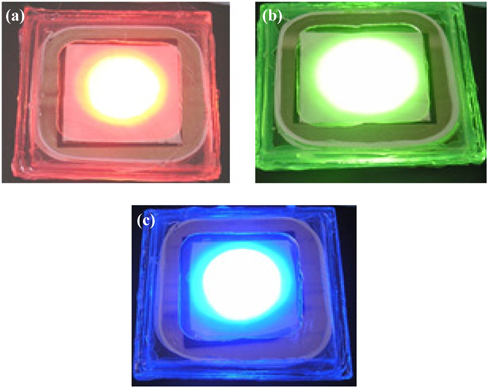
Figure 4 shows light emission at different wavelengths from the planar photocathode devices. An anode plate (with red, green, and blue phosphors, respectively) is utilized. For light of desired color wavelengths, the following phosphor materials are used: silver activated ZnS:Ag phosphor for blue [Fig. 4(a)], terbium activated Y2O3:Tb phosphor for red [Fig. 4(b)], and copper activated ZnS:(Cu, Al) for green [Fig. 4(c)]. The phosphor materials are deposited on an ITO layer, which is used to drain the anode current. An aluminum (Al) backing layer was not used in these cases.
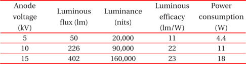
Table 1 shows luminance property values measured as functions of anode voltages from the planar device with a green phosphor screen. Three distinctly different anode voltages (5 kV, 10 kV, 15 kV) were applied for comparison of optical performance. The corresponding electric field strength, which is the bias voltage divided by the gap distance between the photocathode and the anode, was 1 V/μm, 2 V/μm, and 3 V/μm at these three applied voltages, respectively. As expected, all of the measured values are linearly dependent on the applied voltages. This behavior of linear, steep-sloped output is very similar to the characteristics of the cathode ray tube (CRT) and field emission devices. This is likely due to the fact that electron transport to the phosphors for the light emission in this planar device is the same process as that in FEDs.
[Table 1.] Luminance property values measured from the planar device as functions of anode voltages.

Luminance property values measured from the planar device as functions of anode voltages.
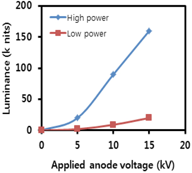
Figure 5 illustrates the measurement of luminance as a function of DC bias voltage for the anode. According to the plot, luminance is strongly dependent on the applied anode voltage. At voltages over 5 kV, luminance increases linearly with respect to the applied voltage, a characteristic of cathodoluminescent phosphors. The measured values under the high power mode are summarized in Table 1. Considering that the luminance of a back-light unit (BLU) is around 10,000 cd/m2 for LCD TV applications, the values obtained were quite large. Even at 5 kV under the low power mode, it was 20,000 cd/m2. The ratio of the electric field strength was 1: 2: 3, based on the applied anode voltage of 5 kV. However, the ratio of the luminance was 1: 4.5: 8, which was much greater than that of the field strength. This indicates that electric field strength can be an important factor for electron acceleration to the phosphors for light emission.
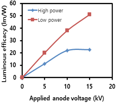
Figure 6 represents the luminous efficacy measured with respect to the applied anode voltages. The luminous efficacy is a measure of brightness efficiency, representing how much light is produced by a lighting source when consuming a unit amount of electric power. This is an important index for the comparison of the energy efficiency of different lighting devices. For example, FEDs with a triode structure using carbon nanotubes (CNT) as field emitters can produce 60 lm/W and OLEDs (organic LEDs) around 40 [9]. The low power mode has a higher value of 50.7 lm/W at 15 kV. Considering that the planar lighting device in this study has a simple diode structure, the measured value is comparable to that of CNT FEDs. On the other hand, the high power mode has 20s lm/W at over 10 kV, which is much lower than that of the low power mode. This indicates that it is appropriate to use a driving scheme with a current limitation in order to produce light efficiently.
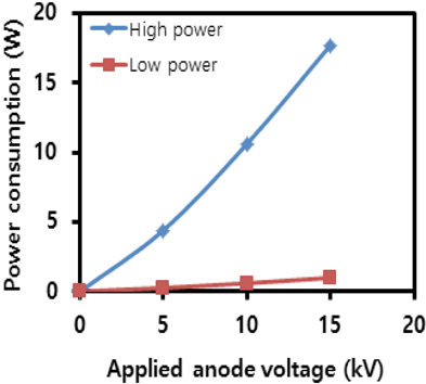
Figure 7 shows the power consumption versus voltage characteristics for light emission of the panel device. As shown, there is a distinct difference between the two modes. The gap increases rapidly with increasing anode voltages. It was more than 10 W at over 10 kV under the high power mode. Considering the panel size, these values are, more or less, high. However, they were less than 1 W under the low power mode. This low power consumption with high voltages is similar to the operating characteristics of the FEDs.
There is a distinct difference between the measured values of major luminous parameters at the same anode voltage in the two modes of operation. If the device is used in more than one environmental condition, a set of measurements is appropriate for each application. The high power mode could be applied to obtain the maximum luminance and light intensity with relatively low luminous efficacy. On the other hand, the low power mode could be applied to obtain maximum luminous efficacy with relatively low power consumption. For planar UV light sources, the high power mode is recommended while the low power mode is appropriate for general planar light source.
We have successfully demonstrated manufacturing of the Cs3Sb mono-alkali photocathode (single alkali metal based photocathode) under inert gas with atmospheric conditions. Planar lighting devices with a simple diode structure were fabricated. One of the key device characteristics is that electron emission is not affected by the electric field strength of the device. The devices showed good brightness, uniformity, and stability without fluctuation over time. They produced an easily directed and controlled stream of light, which make them suitable for a variety of planar lighting device applications.